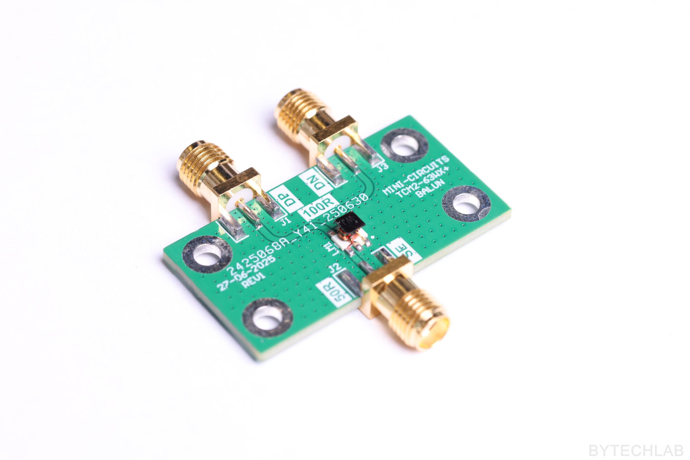
In this post I will show you a very simple Balun PCB (TCM2-63WX+) with a transformer that converts single ended signals to differential signals. Baluns are very useful for many measurements and RF projects.
RF engineering can quickly get very expensive (especially when you go to higher frequencies). Doing RF related projects requires lots of equipment which isn’t cheap. Many expensive components, modules, cables etc. can be made by yourself quite easily, cheaply and quickly. With this project I will start a series of small RF projects that will focus on designing and building useful RF equipment.
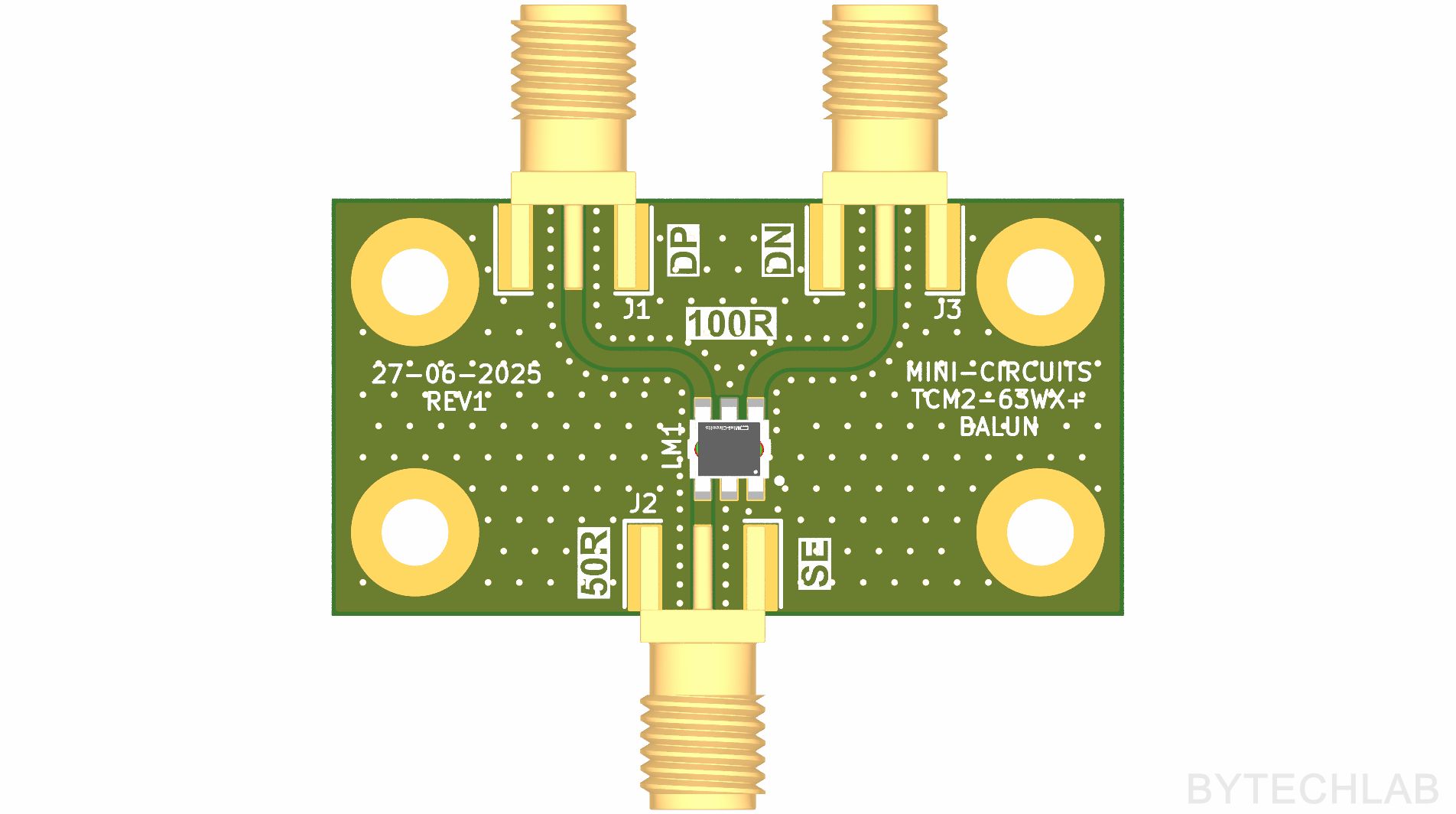
The PCB was designed to operate between 30 and 6000 MHz, it is impedance matched to 50 Ohms SE on every port (50 Ohm SE / 2 x 50=100 Ohm DIFF). The price of each PCB is about 15 USD.
ECAD design
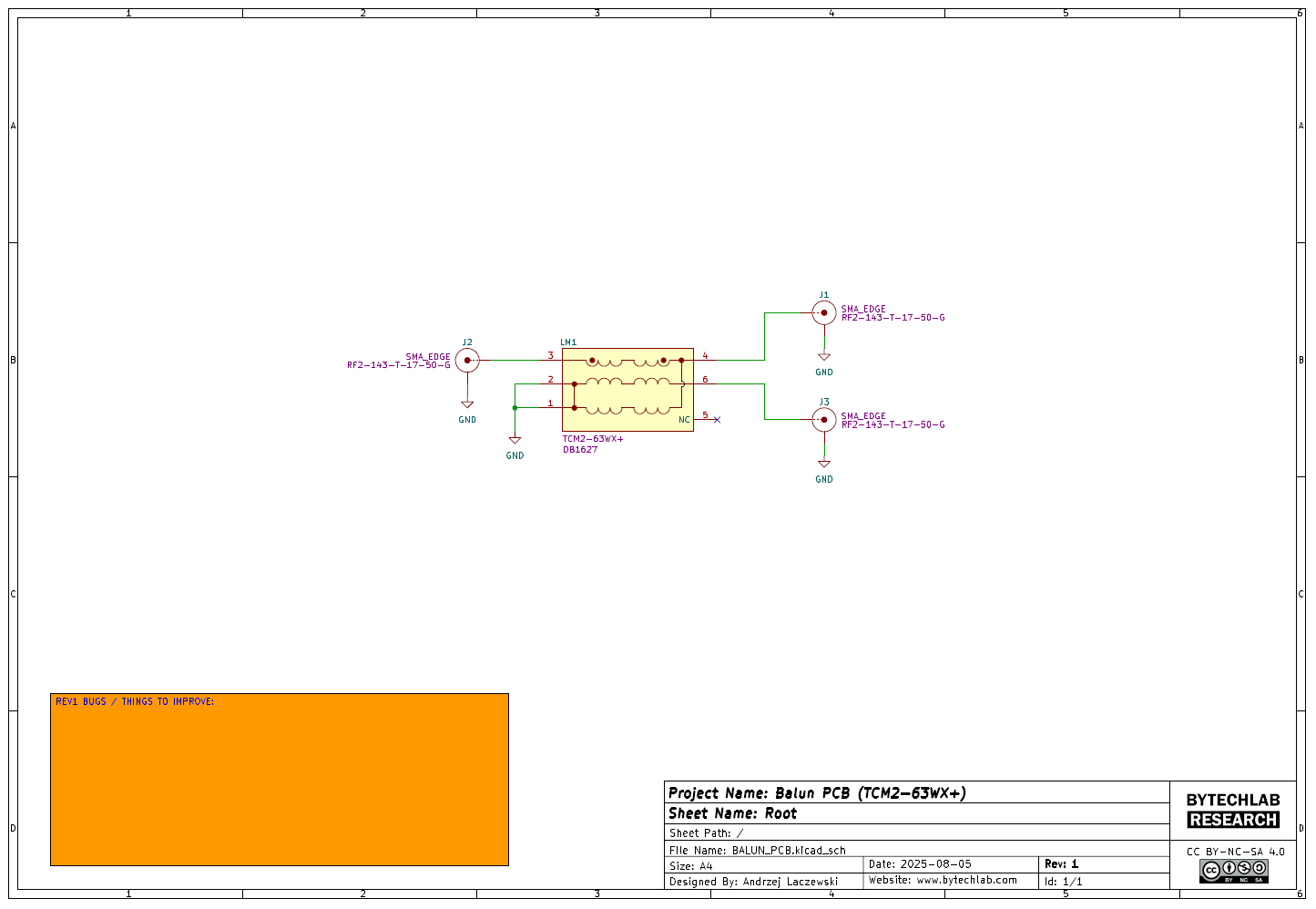
The Balun PCB (TCM2-63WX+) was designed in KiCAD. I have used a standard 1.6mm 2 layer FR4 stackup from JLCPCB to make it as cheap as possible. All transmission lines were routed as coplanar waveguides. The P and N traces were delay matched. I have used MiniCircuits TCM2-63WX+ 1:2 transformer and standard edge launch SMA connectors (Adam Tech RF2-143-T-17-50-G). The TCM2-63WX+ transformer is quite good but it is also quite lossy. The insertion loss can approach values as high as -4dB at 5-6 GHz range according to the Datasheet. Also there will be some loss on the PCB level (quite lossy FR4 was used). This is fine for my current application but I’m sure this may be not a good fit for every application. That’s why I’m planning to do more different PCB’s like this one.
In the GitHub repository (ECAD folder) you can find the following files:
- KiCAD project of the PCB’s,
- Exported GERBER files for manufacturing,
- Exported STEP file of the PCB’s,
- Exported PDF file with schematics and layout,
- Exported BOM and P&P files,

Measurements
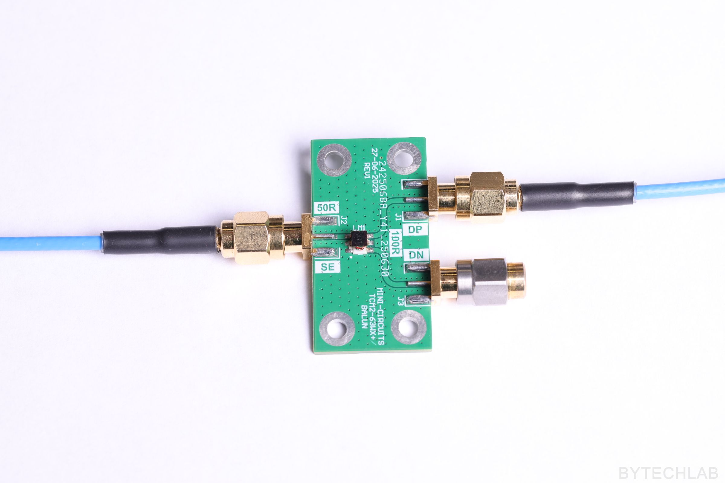
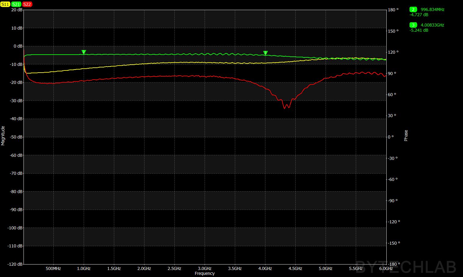
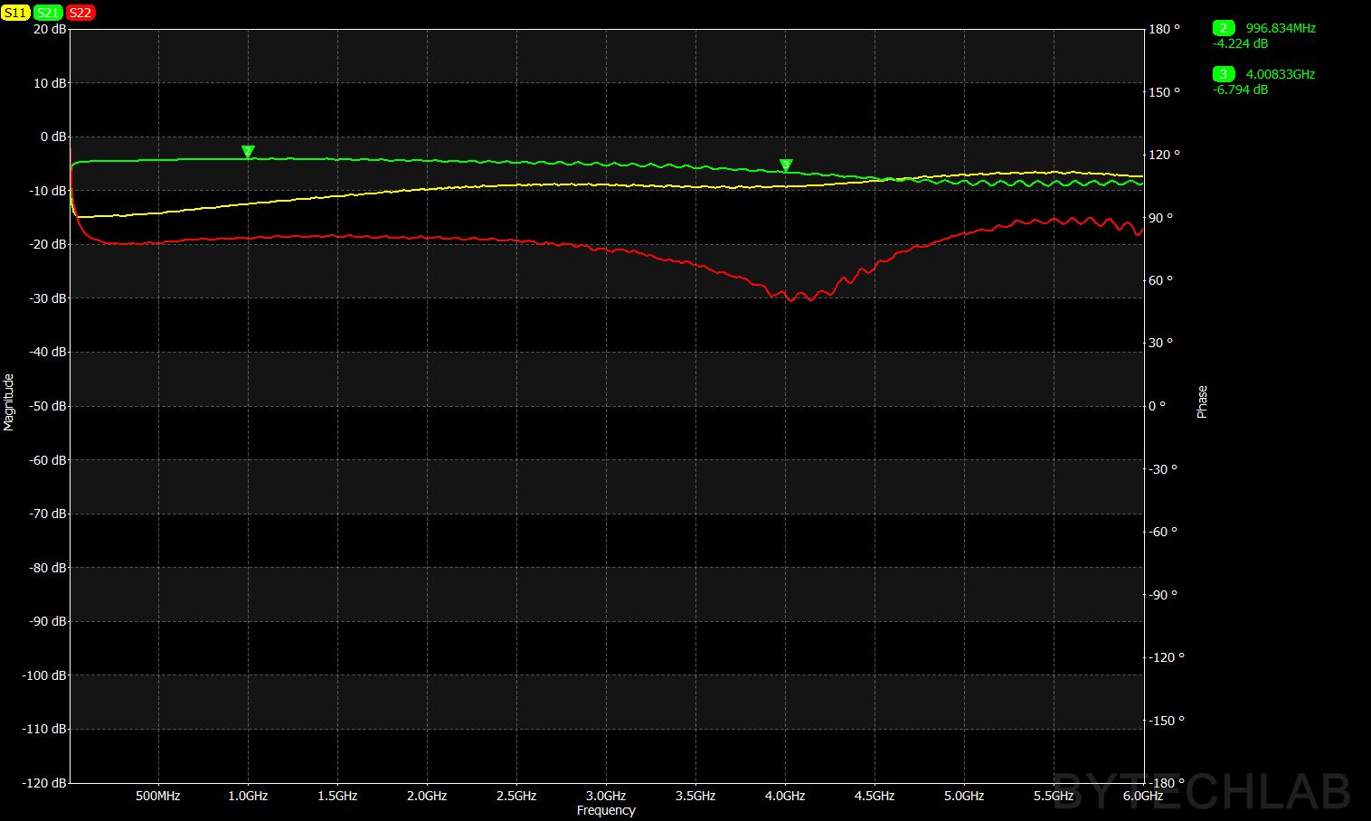
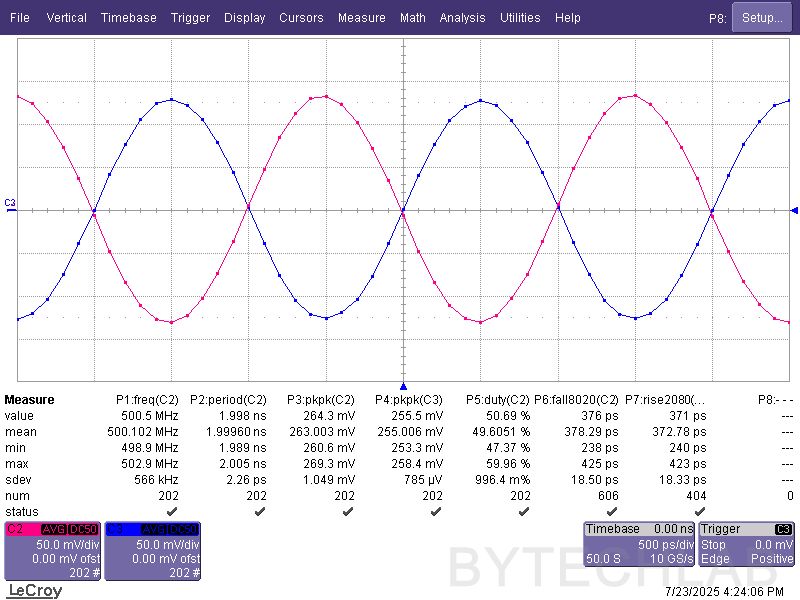
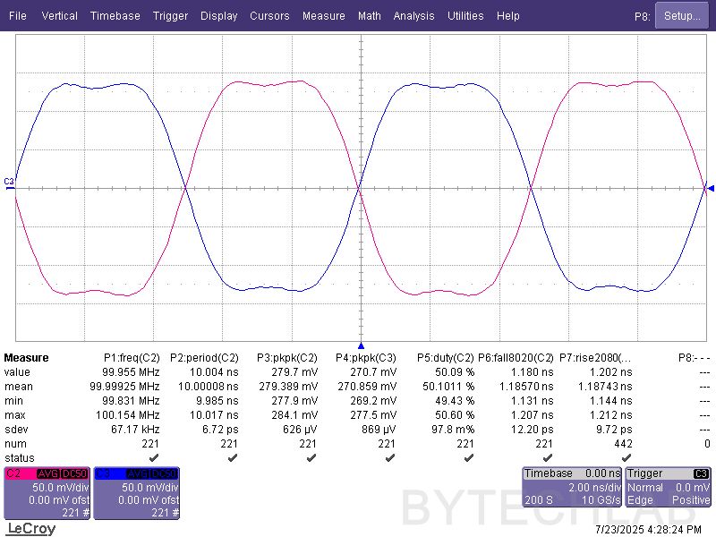
To verify that the whole thing is operating as intended I have made measurements both with the VNA (LibreVNA -100kHz to 6GHz ) and high BW oscilloscope (Lecroy Waverunner 6200A – 2 GHz / 10 GSa/s). As you can see on the oscilloscope screens below the balun works as expected, the waveforms look nice (they match the waveforms at the input when considering the shape) but they are attenuated when compared to the input. Also there’s very little phase shift between P and N waveforms which is good of course.
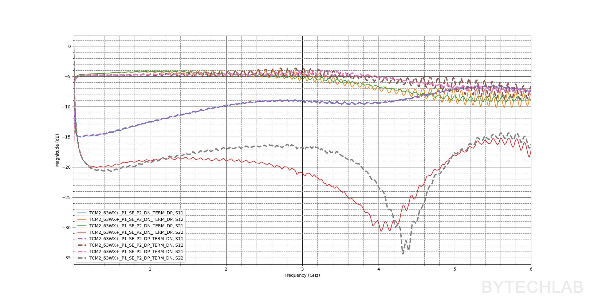
To measure 3 port device with 2 port VNA I have done 2 separate measurements (third port was terminated to 50 Ohms). The two port S-Parameters of SE<->DN and SE<->DP match each other quite well. There is some mismatch of insertion loss between DP and DN at frequencies above 3 GHz. Also the shape of |S22| is not matched perfectly between DP and DN ports (this is fine because the impedance matching is very good anyway). All of the mismatches and other impairments are caused by the non – ideal RF transformer of course. It is good but not perfect. If you want to analyze this further (for example check the exact phase mismatch) you can find the two-port touchstone files in the Github repository.