
This post together with previous antenna related posts is a introduction to a open-source library of wide-band general purpose antennas that I’m planning to create. I will share all information’s about the design process together with detailed electromagnetic simulations results, measurements and assembly instructions so that anyone with basic engineering knowledge will be able to replicate my results. In this post I will show you how I have designed and built PCB Log Periodic Antenna, this is a very well known antenna. There are lots of designs available on the internet.
You can easily purchase one of these antennas commercially. The main problem with these is that you can either purchase very cheap ones (without any simulation results, measurements or design files) or very expensive calibrated, simulated, and measured ones. This design sits somewhere between these two categories. The cost to build antenna presented in this post is about 20-30 USD.
1) Research & Simplified parametric EM simulations
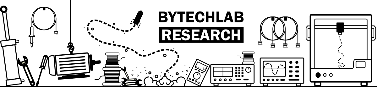
As always I have started the design process with basic research to find useful papers, books and other content on the web. I have found that this paper: [2] “Design a Compact Printed Log-Periodic Biconical Dipole Array Antenna for EMC Measurements” will be very useful during the design process. I have quickly created a simplified parametric model to experiment with this antenna and fine tune all dimensions to get best possible performance out of this antenna architecture. I have chosen to use basic 1.6mm FR4 2 layer PCB laminate from JLCPCB (It can be manufactured for very low price). Unfortunately using cheap FR4 laminate comes at a cost – the antenna efficiency will suffer a little from this choice at higher frequencies.
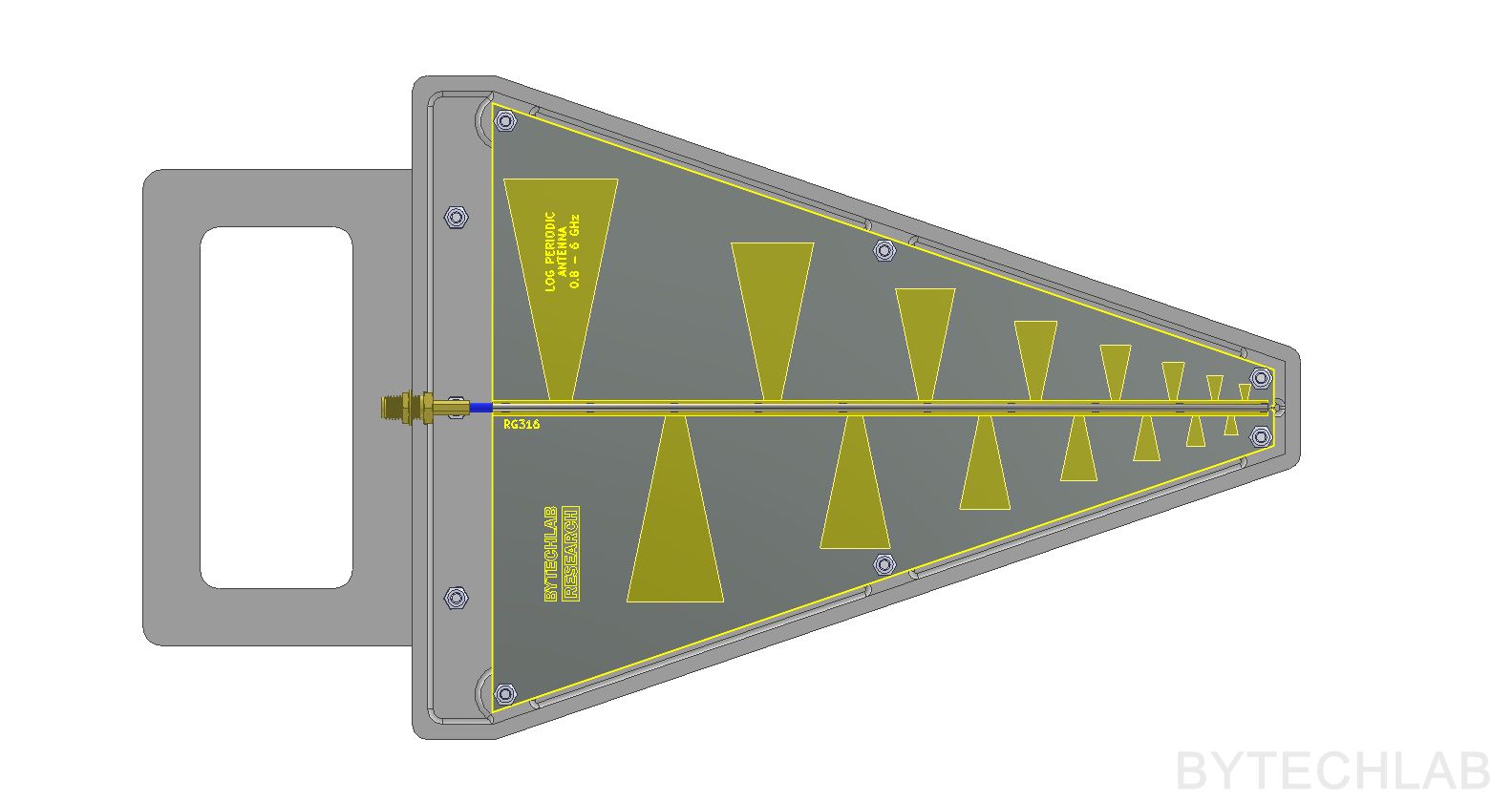
I have chosen to use bow-tie shaped dipoles instead of strip shaped dipoles to improve overall performance of the antenna (each bow-tie dipole is a little more wide-band and has flatter impedance profile than a strip shaped dipole). For initial simulations I have simply added a 50 Ohm lumped port between top and bottom copper layers to feed the antenna. Later this port will be replaced with real coaxial feed.
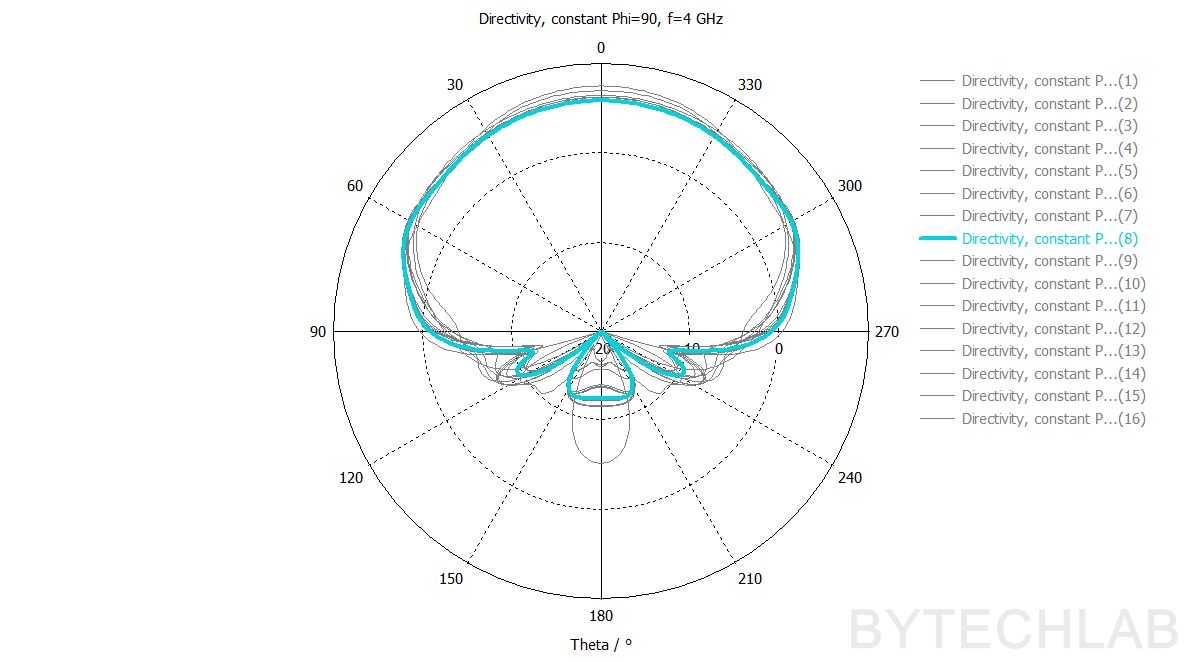

With use of parametric simulations I have fine tuned all of the dimensions to squeeze out the best possible performance out of this architecture. I was able to get very stable beam with small side-lobes and a great impedance matching ( better than -10 dB) in the whole operating band. The antenna directivity is about 6 dBi in the whole operating band.
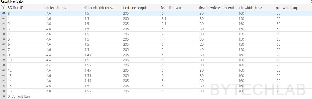
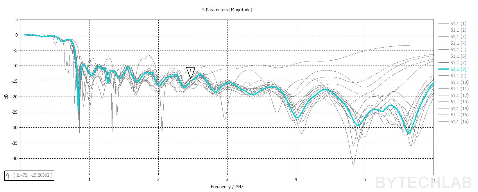
As a last step before I move further with the design I have checked how the whole antenna is sensitive to FR4 dielectric thickness variation as well as dielectric constant variation. I have simulated all combinations of PCB thickness and dielectric constant set to the following values ( = 1.45, 1.5, 1.55 mm & = 4.4, 4.6, 4.8). Based on the simulation results I was able to tell that changing these parameters in the presented range has little to no influence on antenna performance (for ex. take look at the chart above).
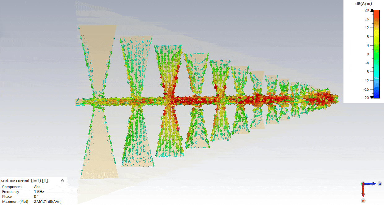
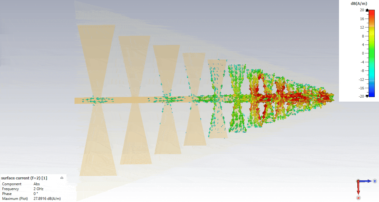
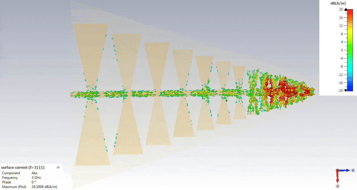
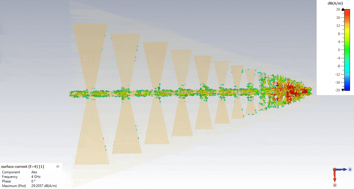
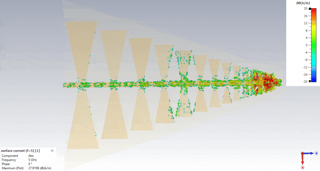
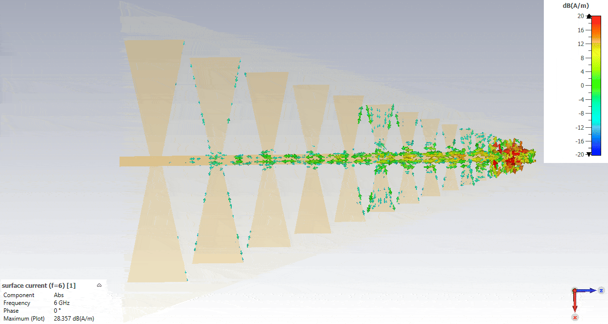
On the animations above you can see the surface current distribution for frequencies equal 1,2,3,4,5 and 6 GHz. These animations are very helpful in analyzing the antenna behavior and understanding the principle of operation. You can see that active region (area where dipole resonate or are close to the resonance) moves from the large dipoles to the smaller ones as the frequency increases. Shorter dipoles in front of active region act as directors (they enhance the forward radiation) and the longer dipoles at the back of active region act as reflectors (they reduce backward radiation).
2) Coaxial feed optimization
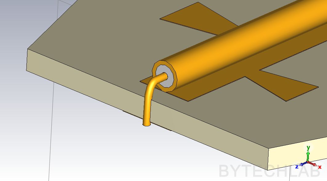
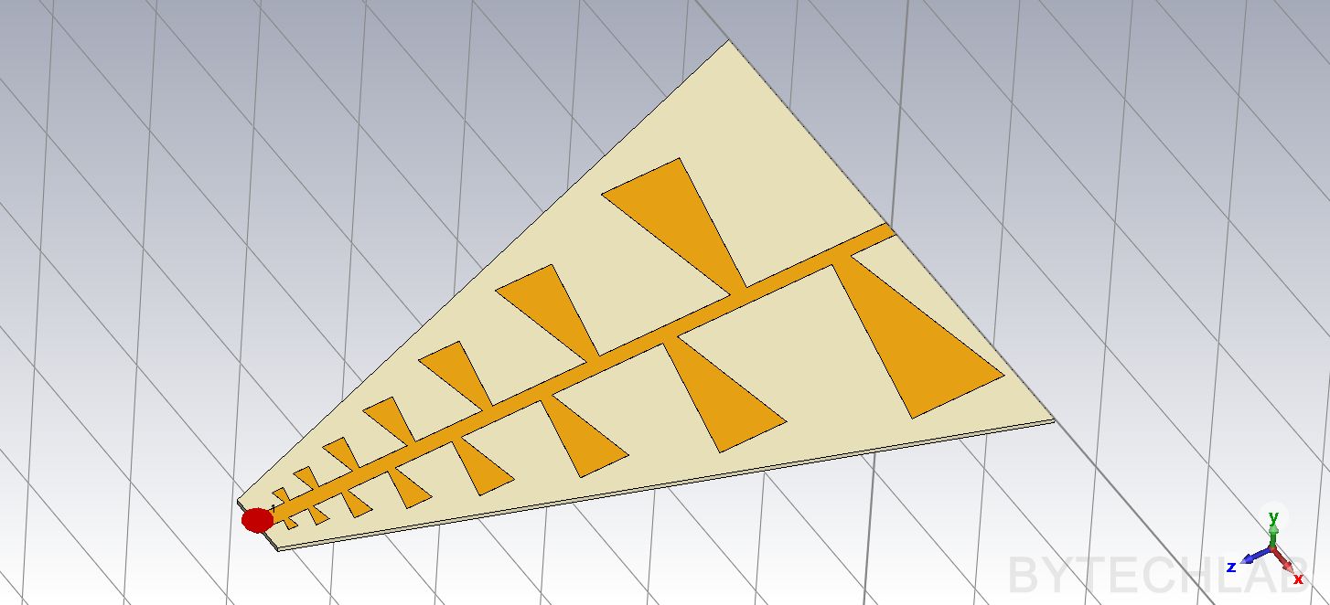
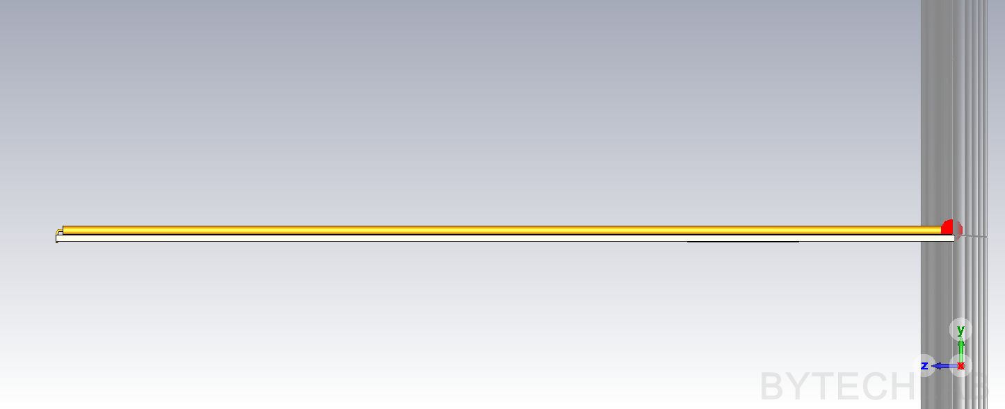
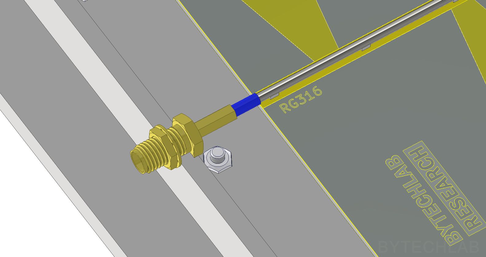
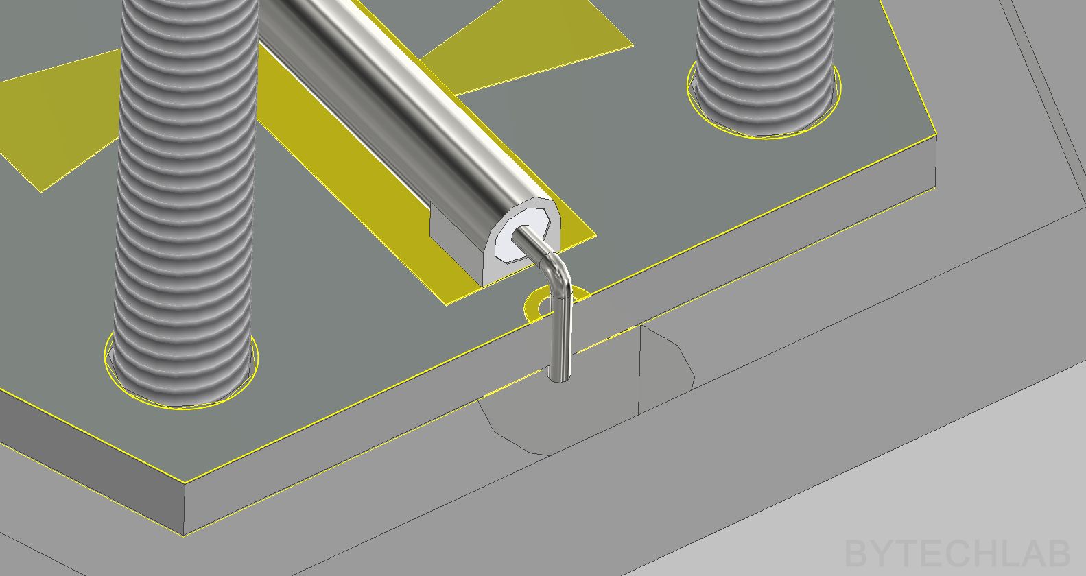
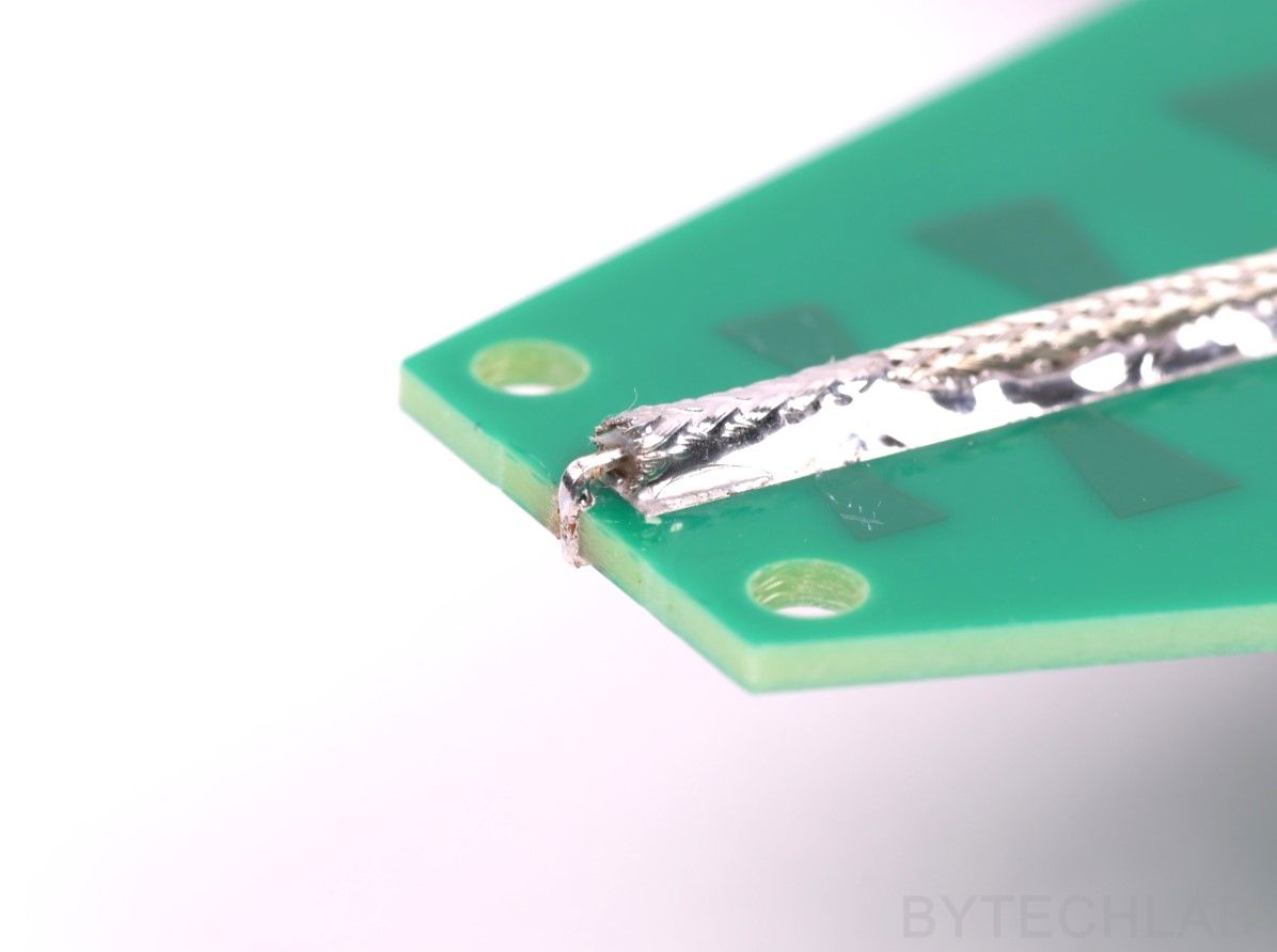
As the next step I have added a fully parametric coaxial feed to the antenna model to fine tune all dimensions to get best possible performance. I have used a RG316 low loss coaxial cable for this purpose. If you want to use this antenna without 3D printed enclosure you can use a semi-rigid coaxial cable so that you can use it both for feeding the antenna and mounting it mechanically to your equipment.
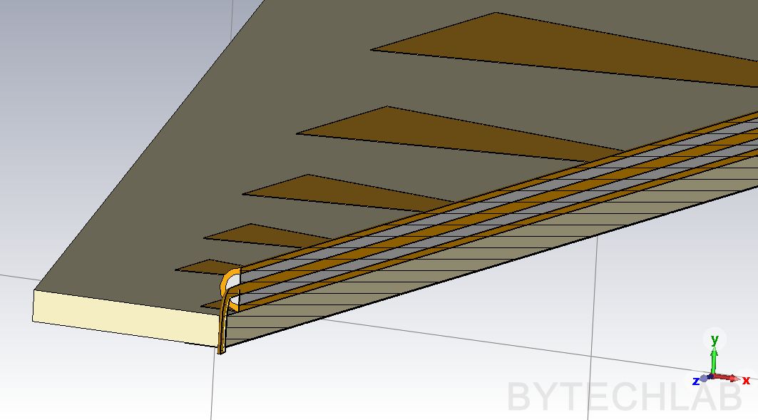
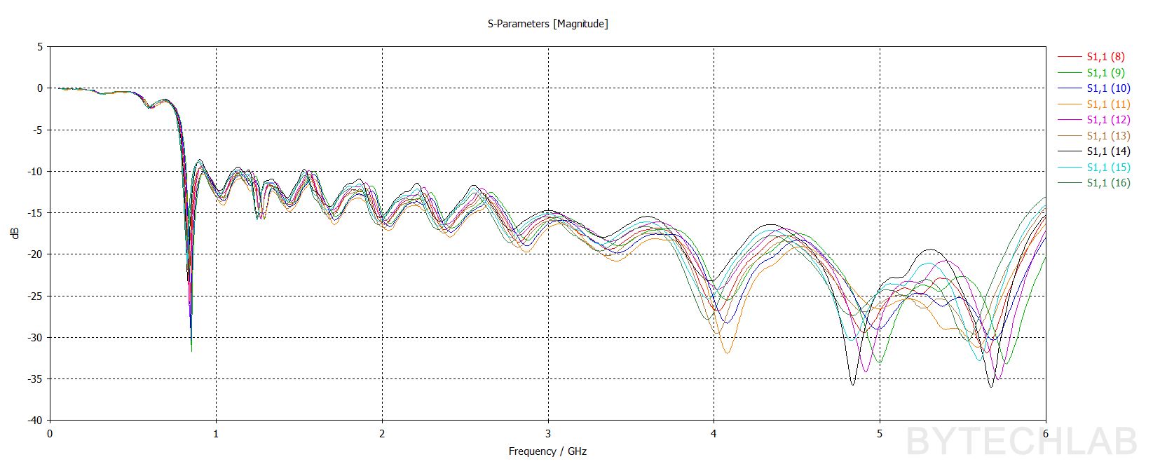
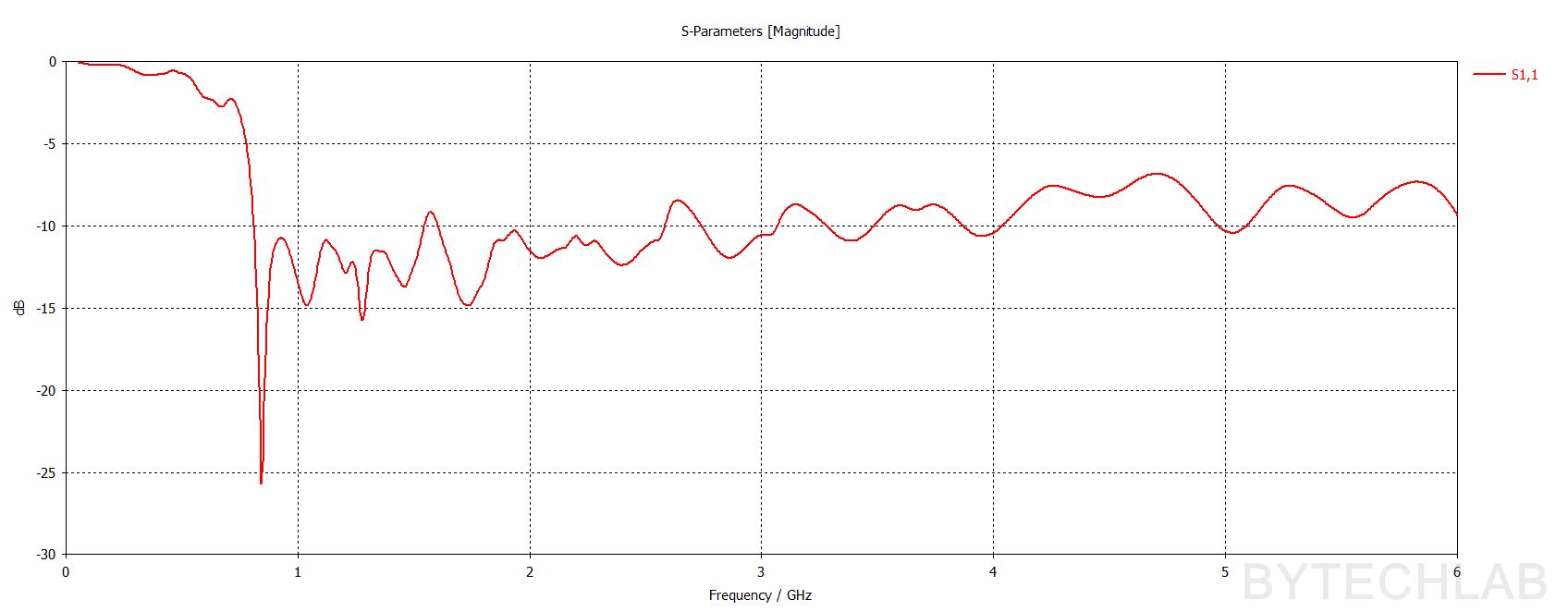
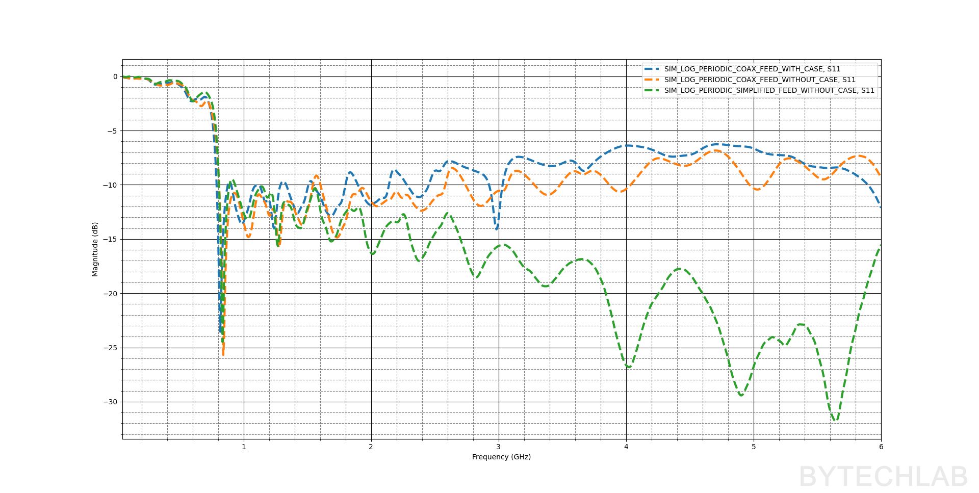
As I quickly figured it out, the feeding structure is a very important part of this antenna. Improper feeding technique can drastically degrade the overall antenna performance (degraded impedance matching, beam tilt, large side lobes, etc.). The most important part of this feeding structure is to basically keep the coax center conductor that comes out at the tip of the antenna as short as possible. You can see that the parameter got worse at higher frequencies due to using this feeding structure. I wasn’t able to optimize this further (It’s good enough for me at the moment).
3) MCAD & ECAD design
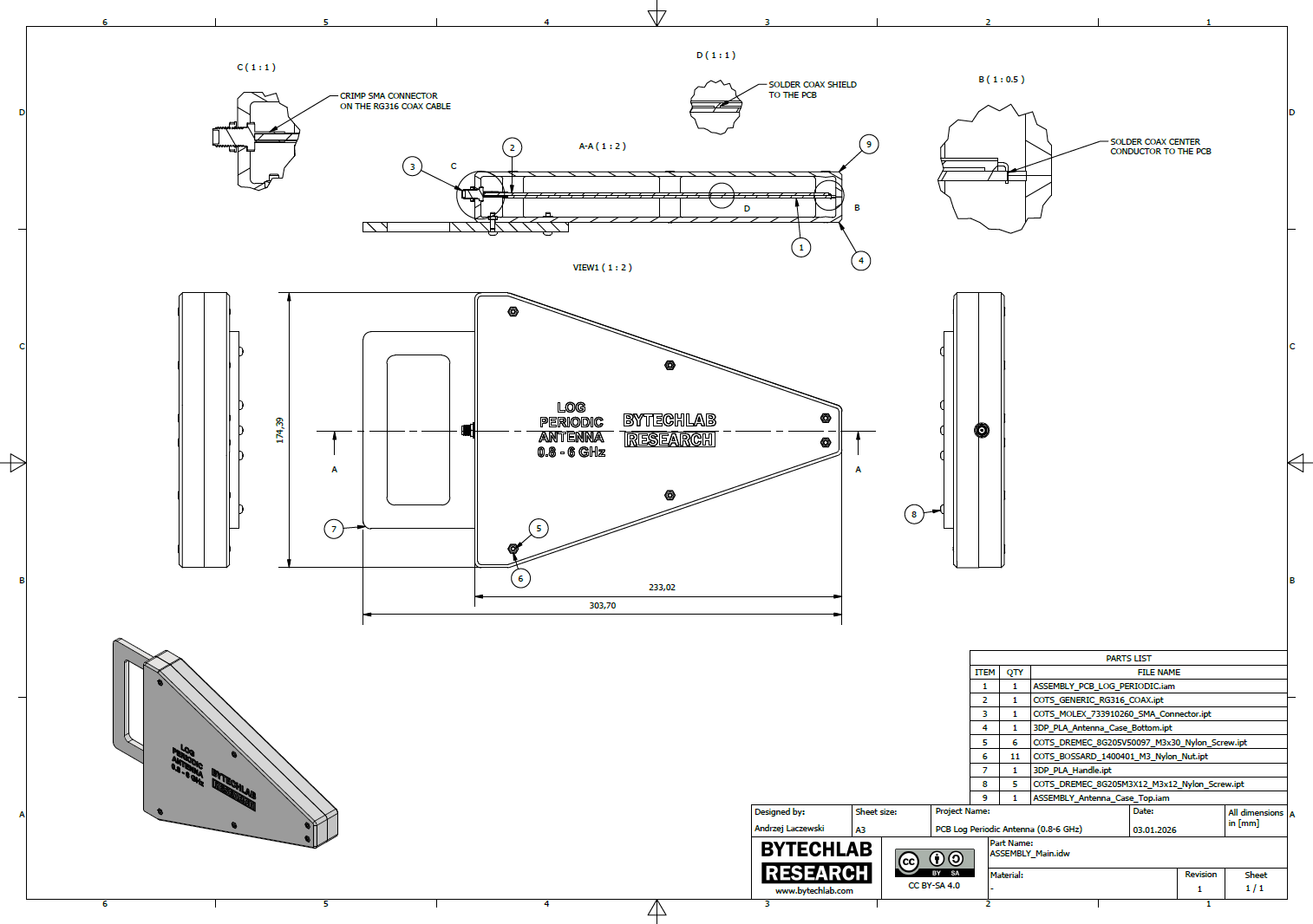
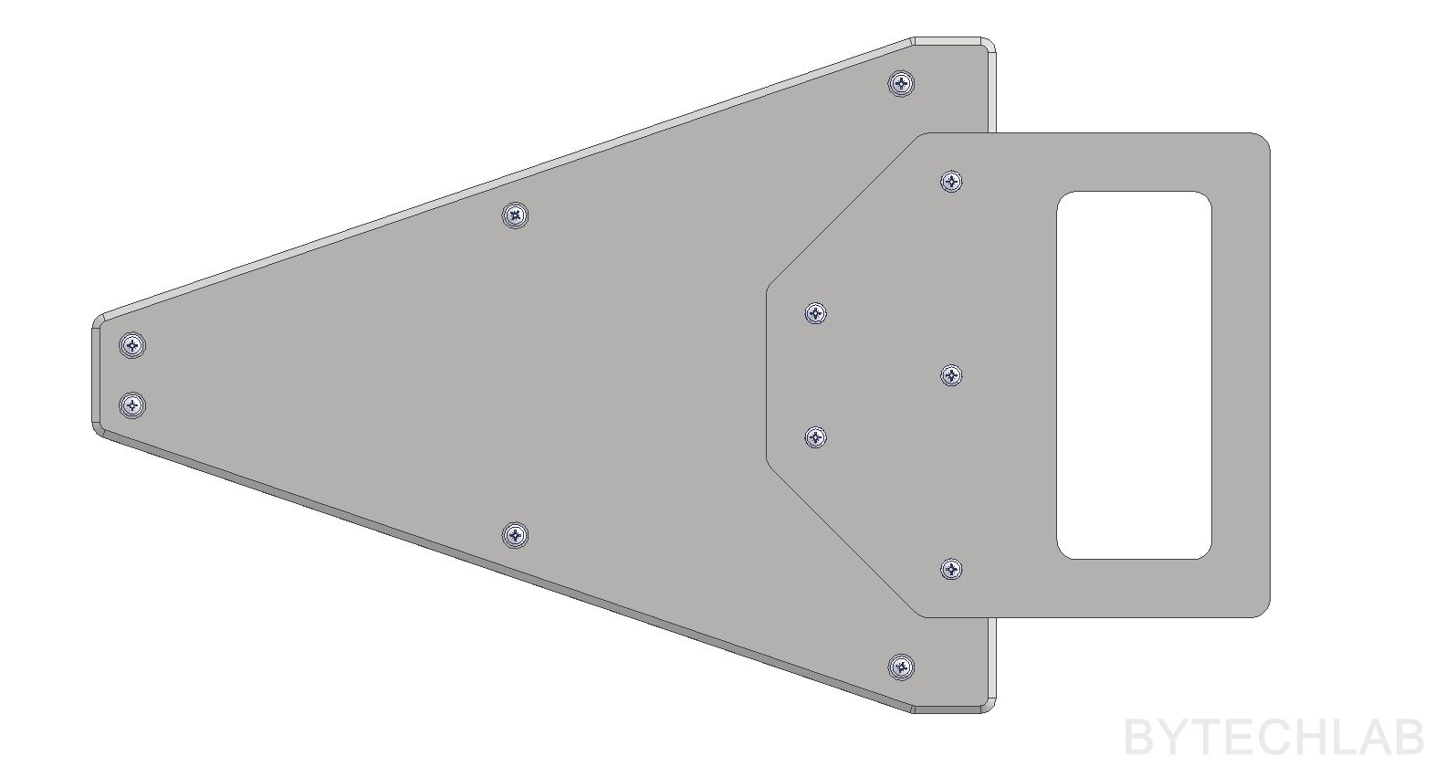
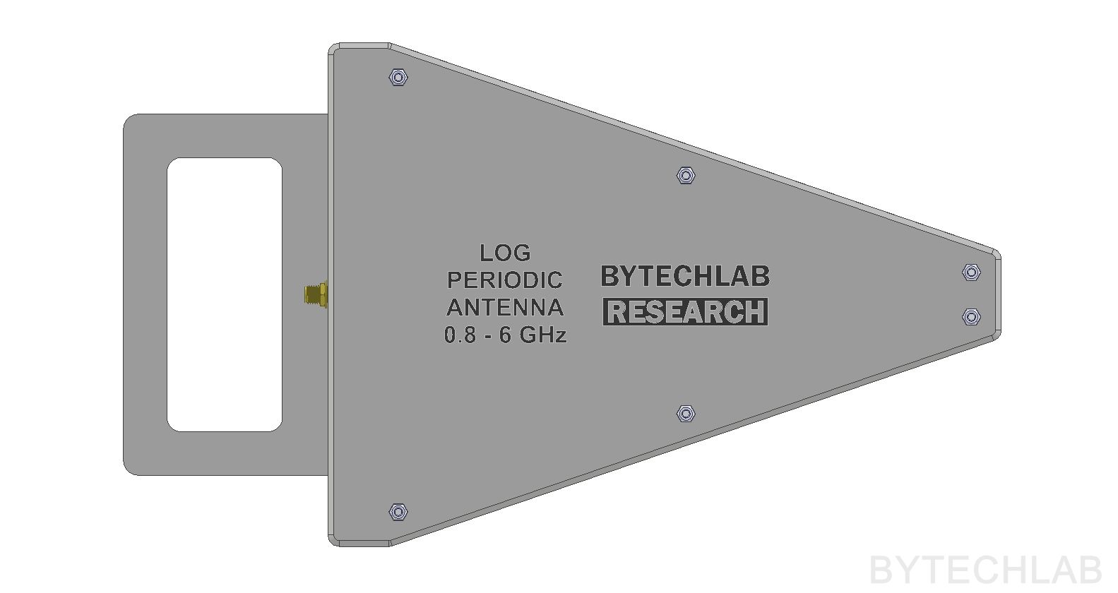
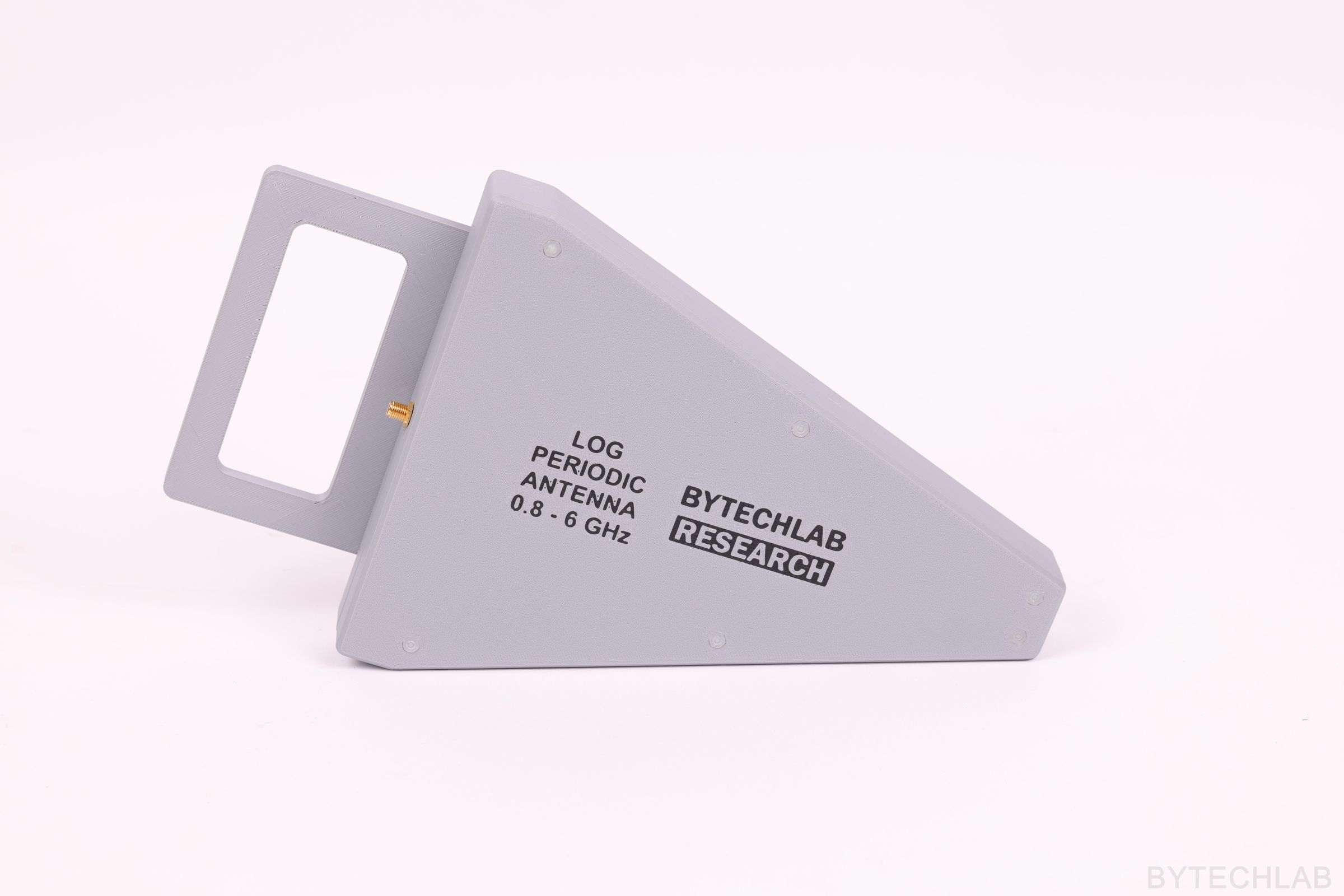
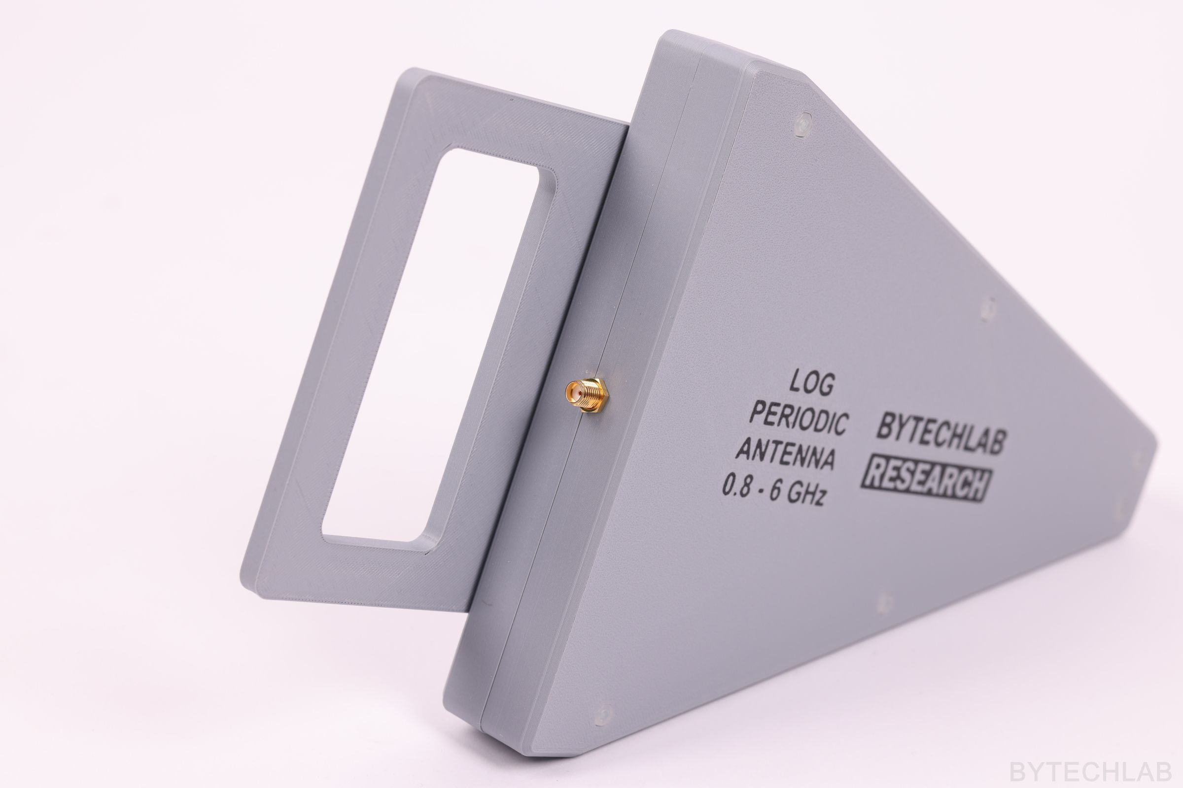
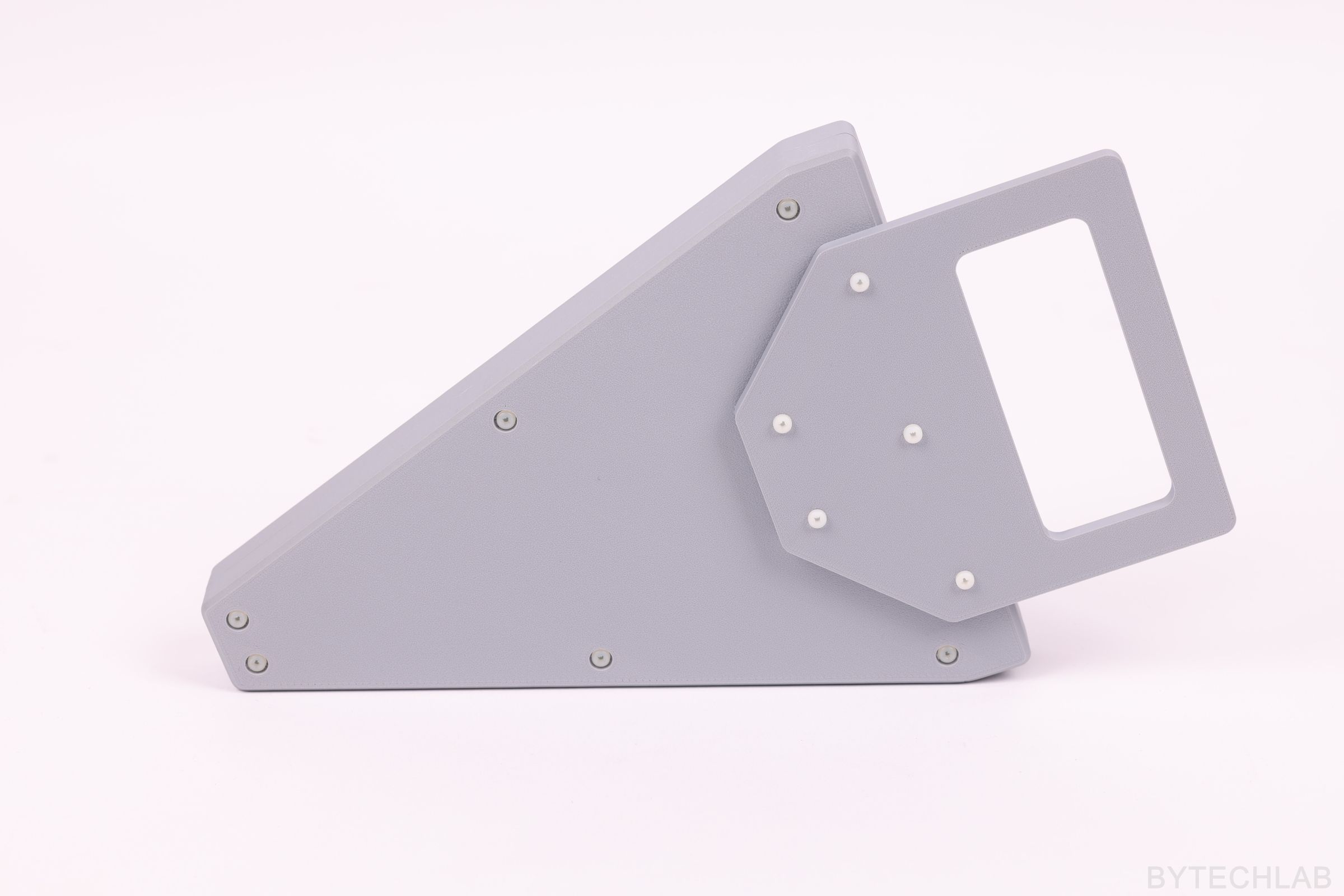
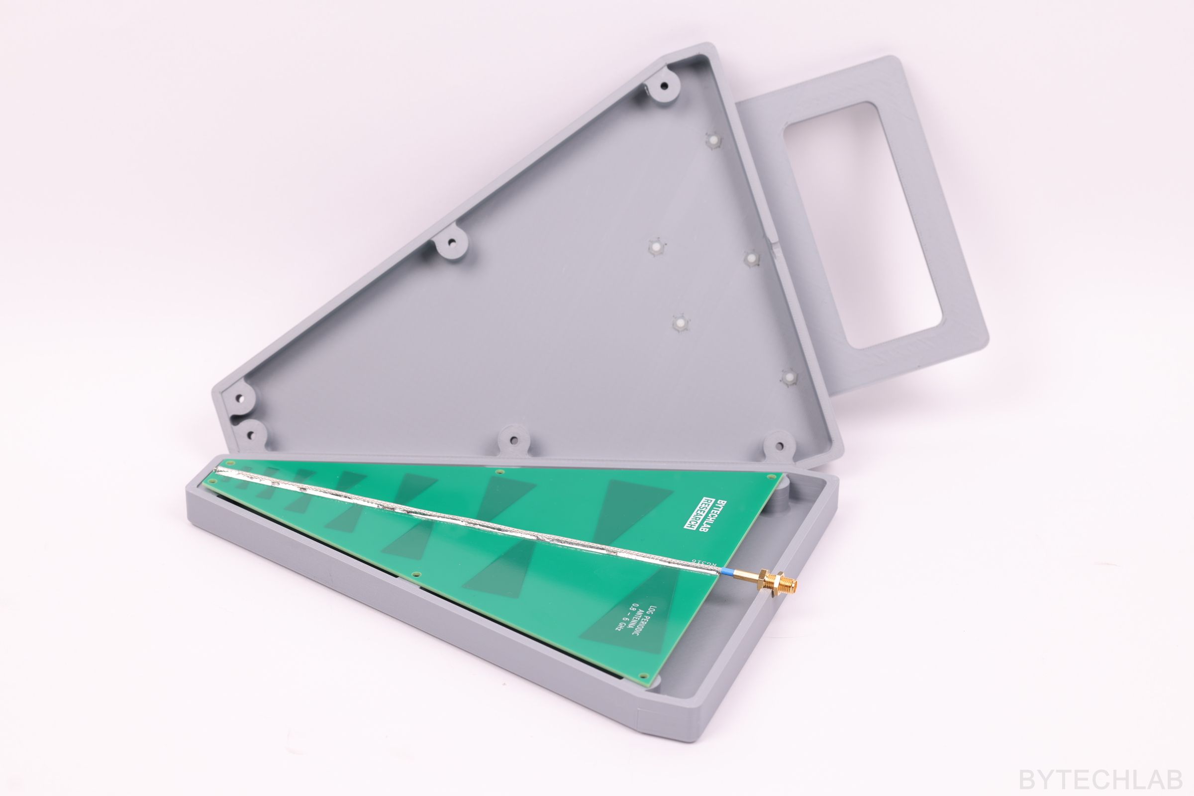
To protect the antenna itself from mechanical damage and add mechanical mounting system / handle to use the antenna outdoors I have decided to design a simple 3D printed enclosure. The enclosure was designed in the way to reduce the influence on the antenna performance as much as possible. The 3D printed enclosure is assembled together with use of M3 Nylon screws.
To assemble the whole antenna you simply need to:
- Order PCB’s from JLCPCB,
- Prepare and solder coaxial cable to the PCB and crimp the SMA connector,
- 3D print the antenna case and assemble everything together
In the GitHub repository (MCAD folder) you can find the following files:
- Autodesk Inventor project of PCB Log Periodic Antenna enclousure,
- Exported STL files for 3D printing,
- Exported STEP file of the whole assembly,
- Exported PDF file with assembly drawing, BOM and assembly instructions,
- Exported assembly renders,
In the GitHub repository (ECAD folder) you can find the following files:
- KiCAD project of the PCB Log Periodic Antenna,
- Exported GERBER files for manufacturing,
- Exported STEP file of the PCB’s,
- Exported PDF file with schematics and layout,
- Exported BOM and P&P files,
4) Final EM simulation
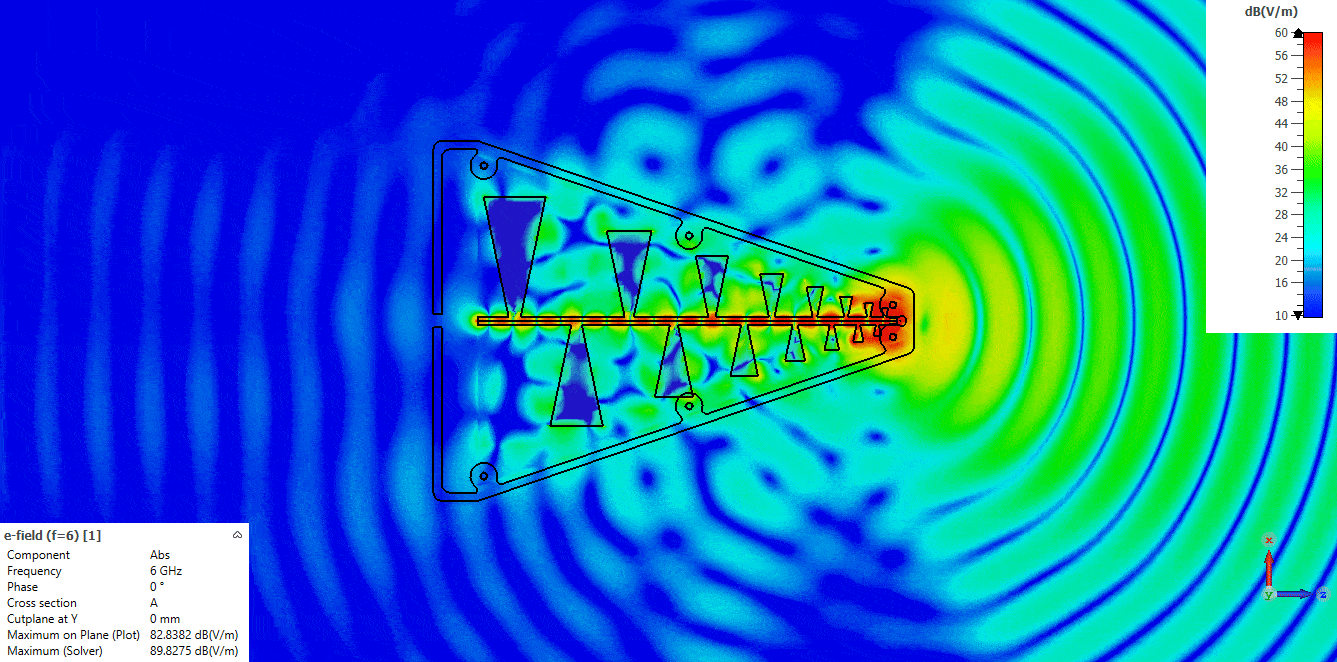
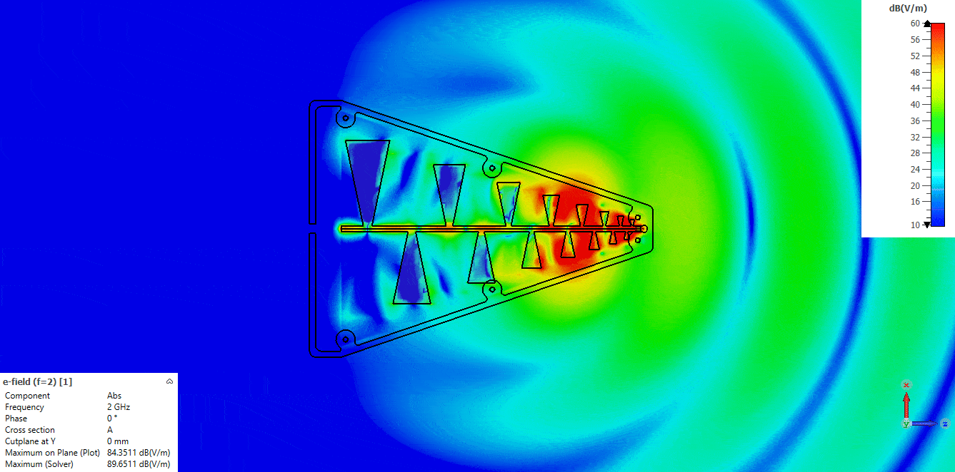
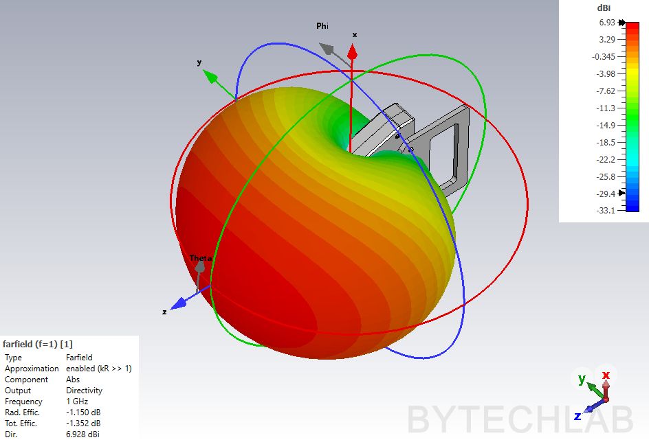
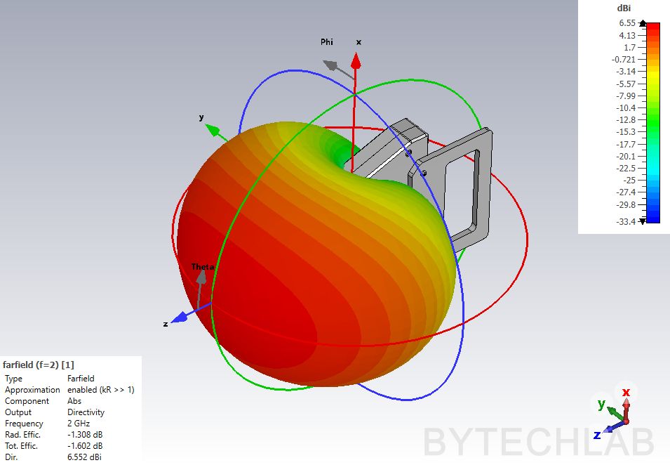
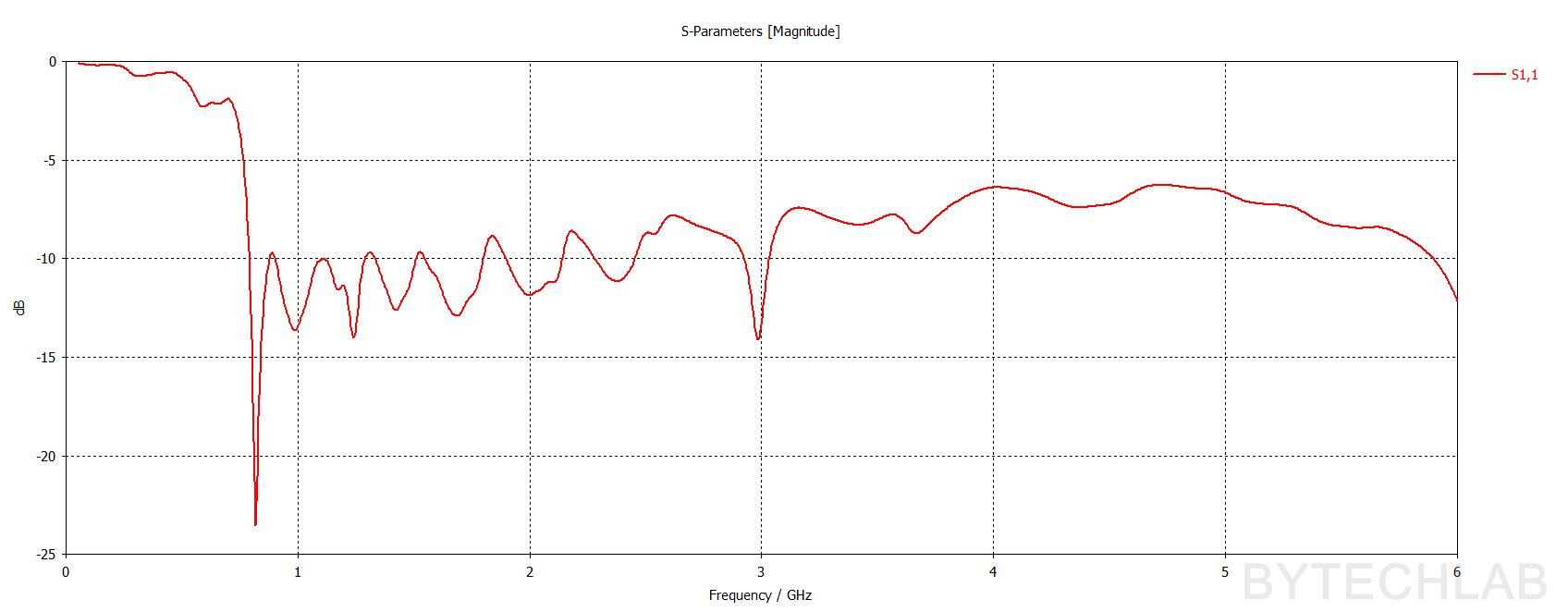
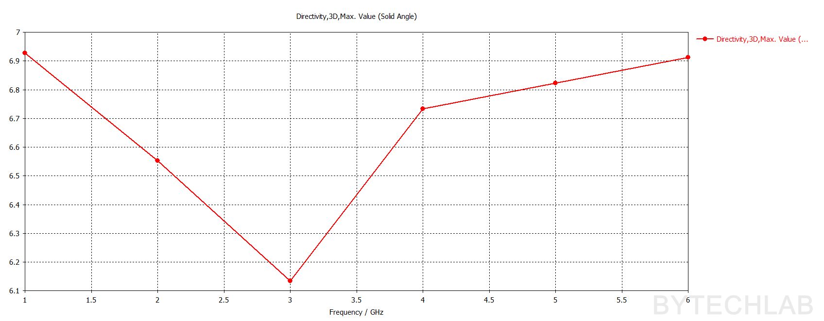
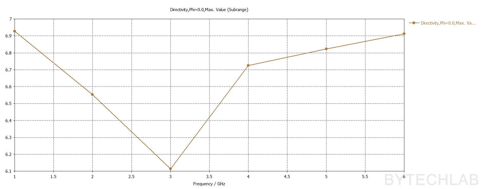
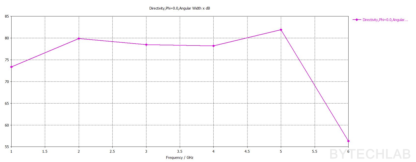
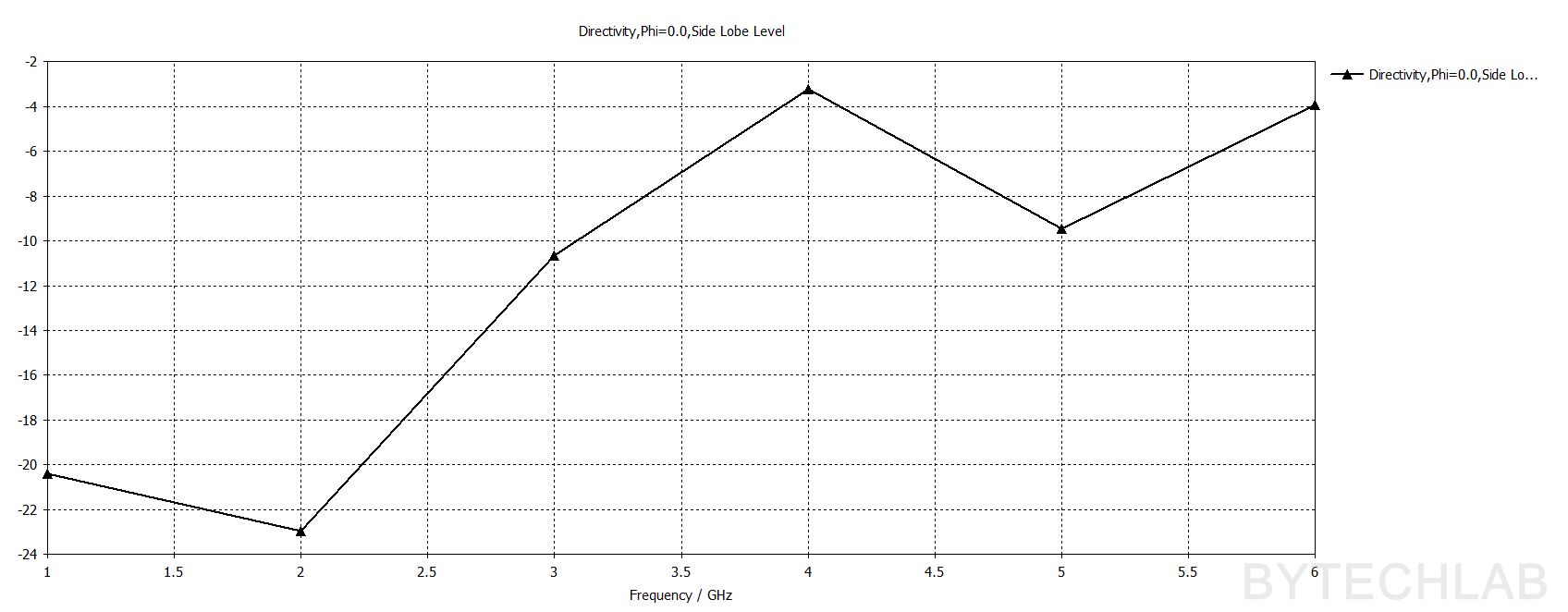
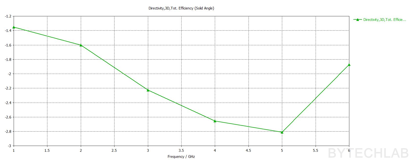
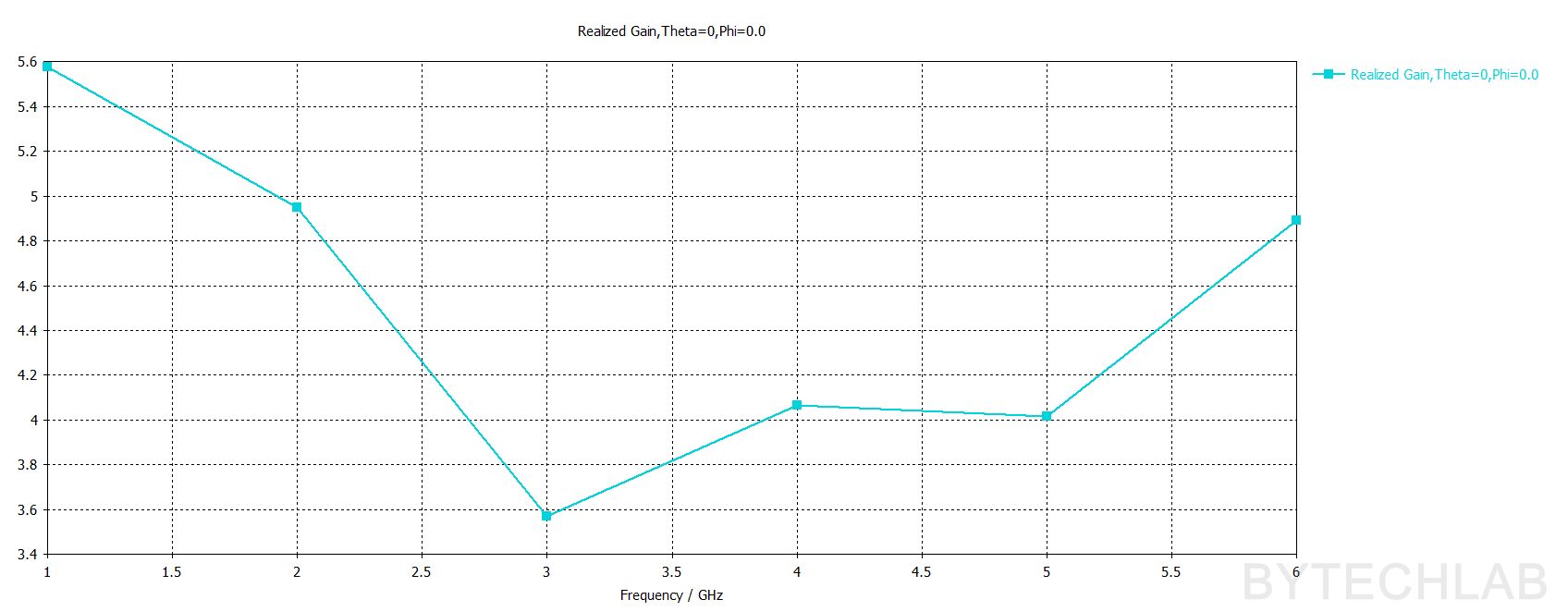
To verify the final design I have exported the whole antenna from Autodesk Inventor and imported it back into CST Studio for final simulation. I have ran full set of simulations to ensure that the antenna will work well in every aspect. Below you can see the 3D far-field renders (directivity). The main beam is very stable in the whole operating frequency range. I was able to achieve about 6 dBi of gain. On above animations you can see the E field propagating though the antenna structure at 2 and 6 GHz. The directional behavior is clearly visible (directors/reflectors).
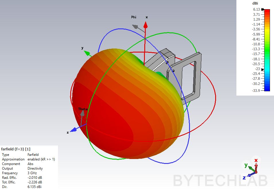
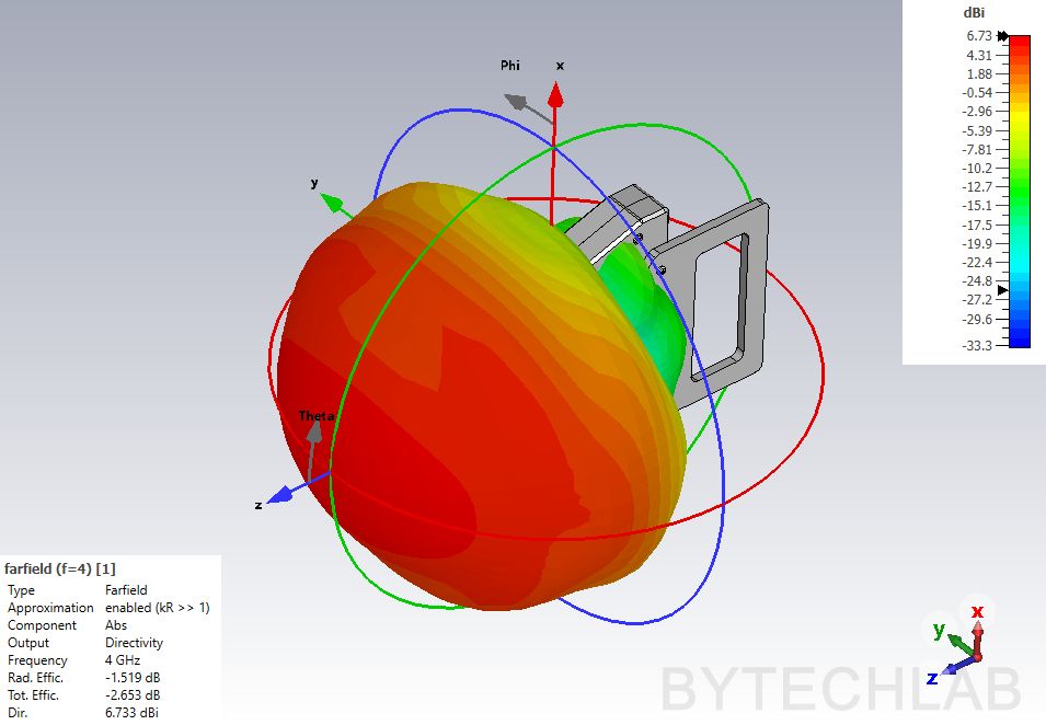
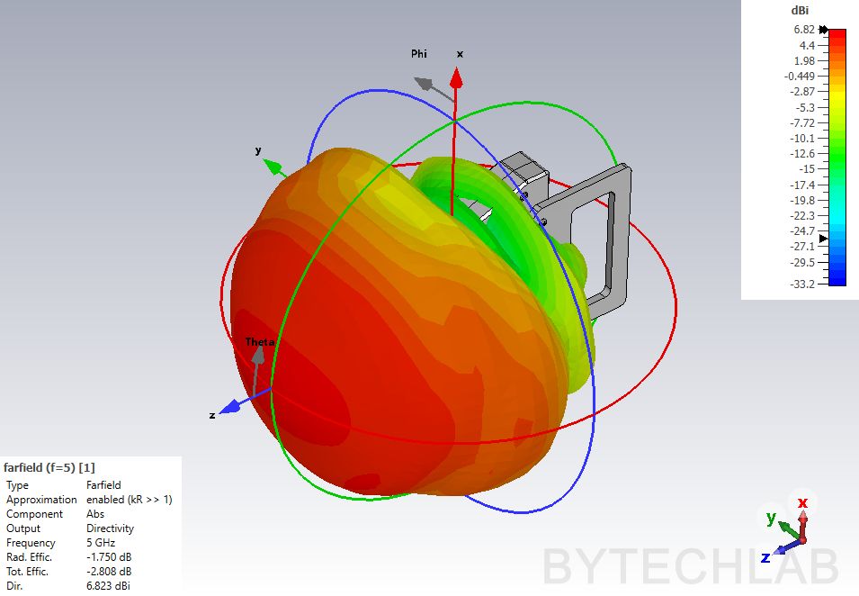
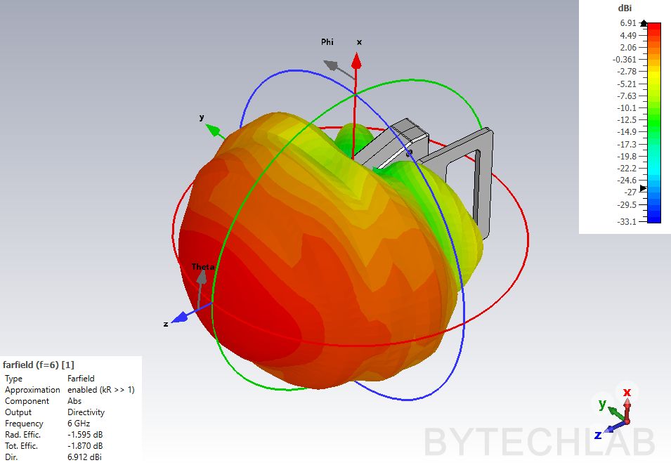
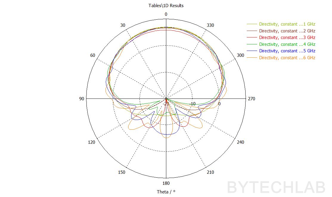
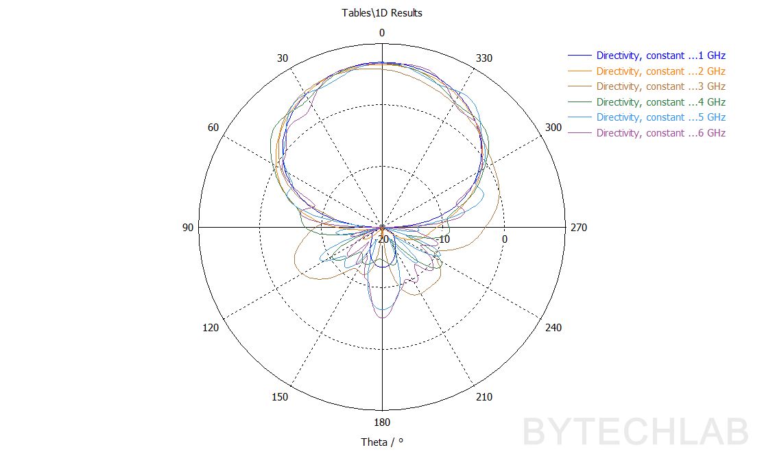
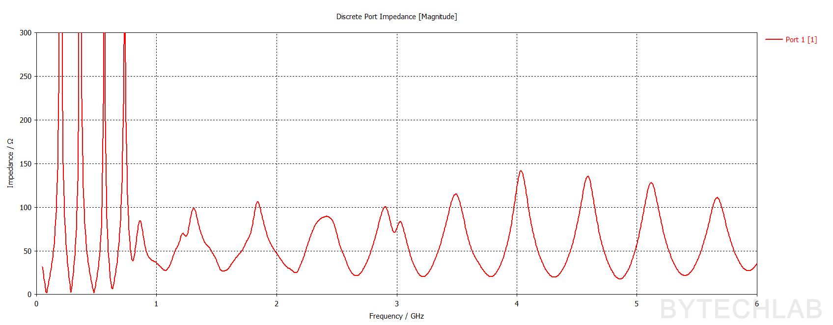
Below you can see also other antenna characteristics such as: Directivity -2D farfield cuts (phi=0,phi=90),, Port impedance, Directivity Max., Angular width (phi=0), Side lobe level (Phi =0), Total Efficiency, Realized Gain (phi =0, theta=0).
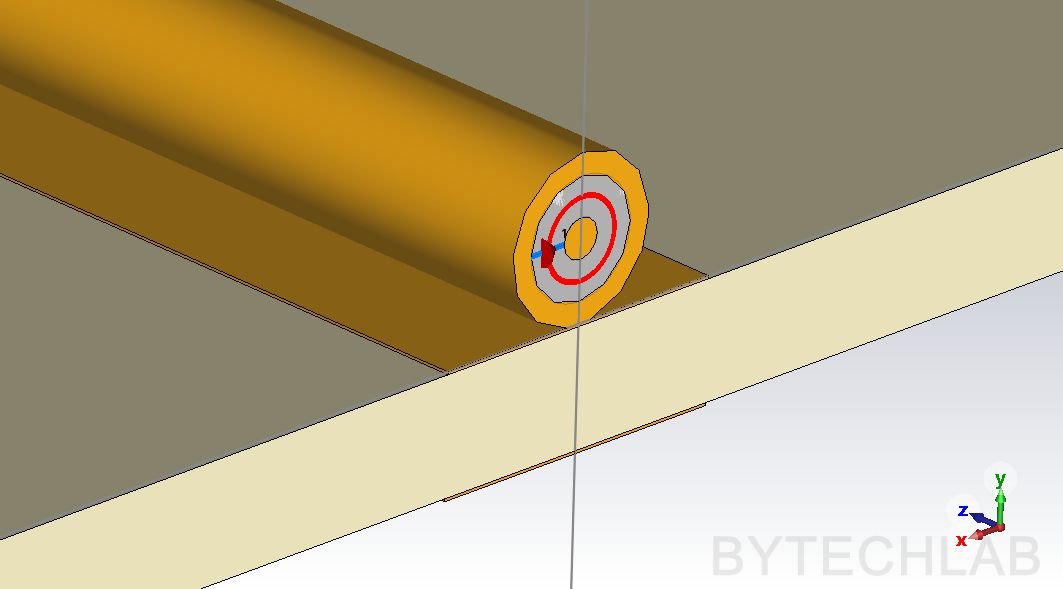
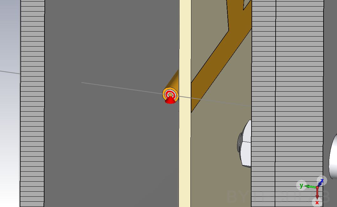
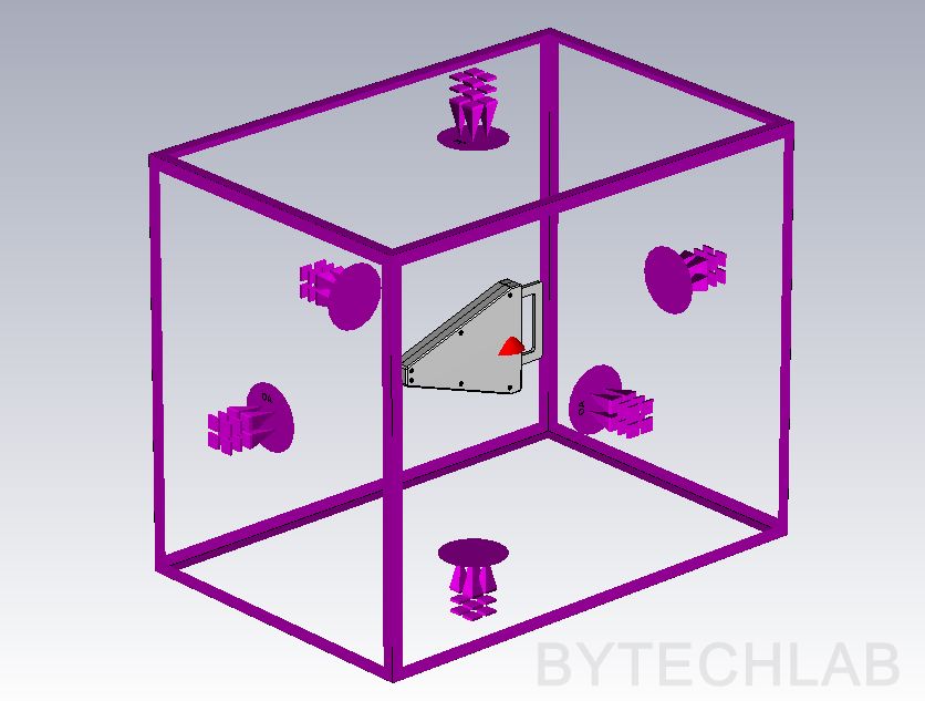
Also on the screens below you can see the port placement and the open boundary box around the antenna:
To visualize the parameter degradation during each design phase I have prepared additional plot. It’s easy to see that using the coaxial feeding structure degraded the at higher frequencies. Adding the 3D printed enclosure degraded the even more. I have optimized the enclosure to impact the antenna performance as little as possible mainly by using low-infill 3D prints ( around 30% ) to reduce the effective of the enclosure.
To make the final simulations I have used the PLA properties for different infill values from this paper: [1] “Analysis of FDM and DLP 3D-Printing Technologies to Prototype Electromagnetic Devices for RFID Applications”. Please note that these values are only a rough estimation – for example my simulation model does not take into account the non-uniform internal structure of the 3D printed parts.
![PCB Log Periodic Antenna - [1] Generic PLA filament properties - Dielectric constant and Loss tan](https://bytechlab.com/content/uploads/2026/01/pcb-log-periodic-antenna-pla-filament-properties.png)
5) 3D printing
The enclosure parts were 3D printed from Bambulab PLA Basic filament on my Bambulab X1C 3D printers. The antenna name as well as BYTECHLAB logo were 3D printed into the enclosure using filament swapping with AMS.
You can find the .3MF file for BambuStudio in the GitHub repository.
Recommended printing settings:
- 0.2 mm layer height,
- BambuLab PLA Basic filament (don’t use a filament that has any conductive additives [carbon fiber, sparkle etc..] ! )
- 30 % rectilinear/grid infill,
- 2 outlines,
- 2 solid top/bottom layers,
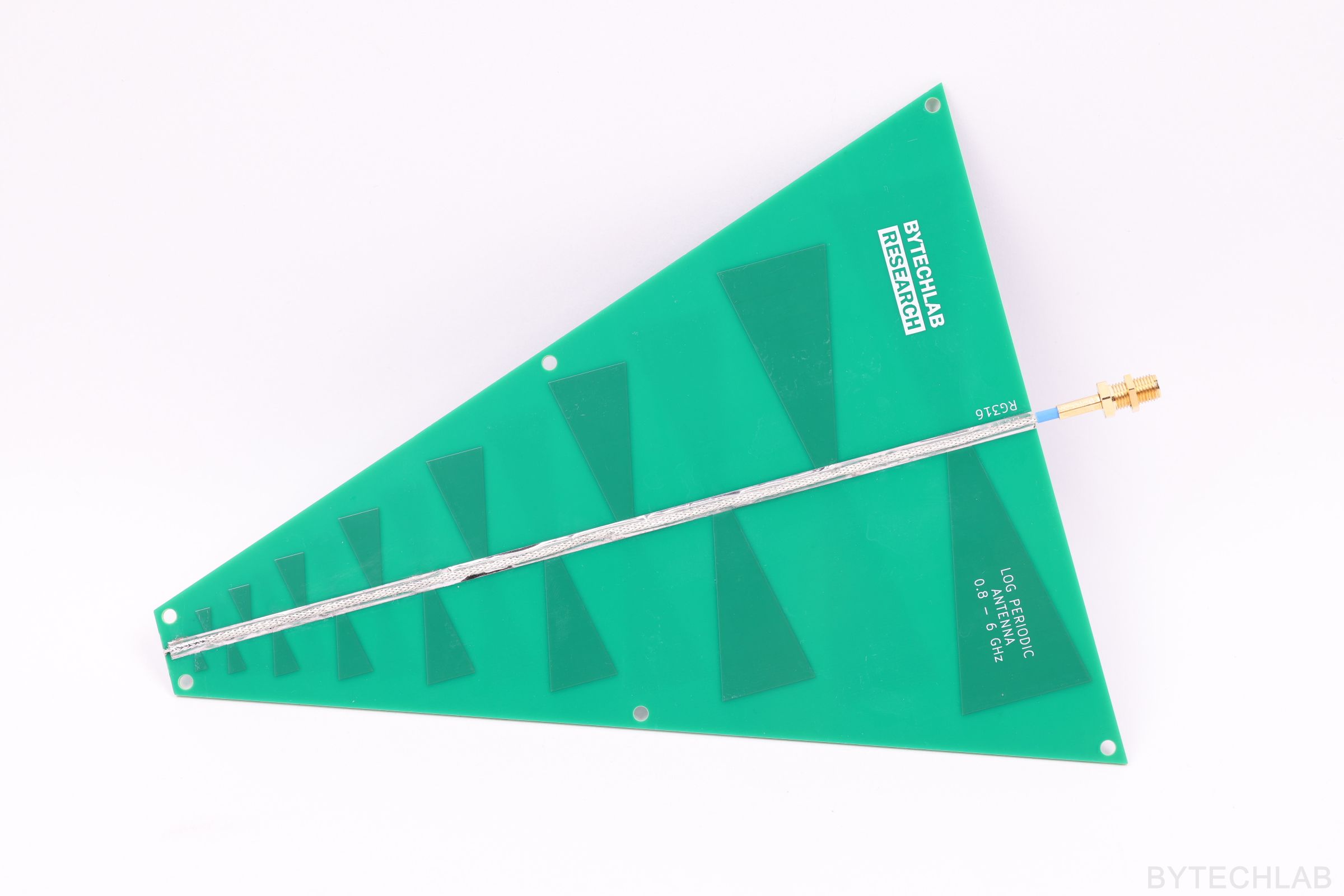
6) Photos
7) Measurements

Measurements were performed with use of my LibreVNA. Antenna was placed on EM absorber sheets in my lab as far as possible from other objects. This measurement methodology is not ideal but it’s good enough for now, I will probably repeat these measurements when I will get access to better equipment (like anechoic chamber). The correlation between measurement and simulation is very good for bare PCB’s. The correlation is a little bit worse for antennas with 3D printed enclosures. This might happen due to various reasons like poor filament EM model, poor dimensional accuracy, poor EM model of 3D printed parts, non ideal measurement environment, etc.
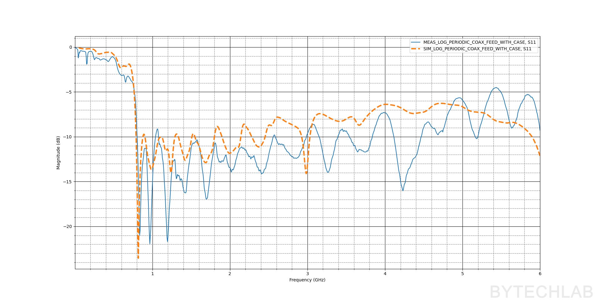
I have also compared the bare PCB’s and PCB with enclosure measurements with each other, The enclosure degrades the parameter a little at higher frequencies as predicted.

Antenna radiation patterns measurements coming soon!
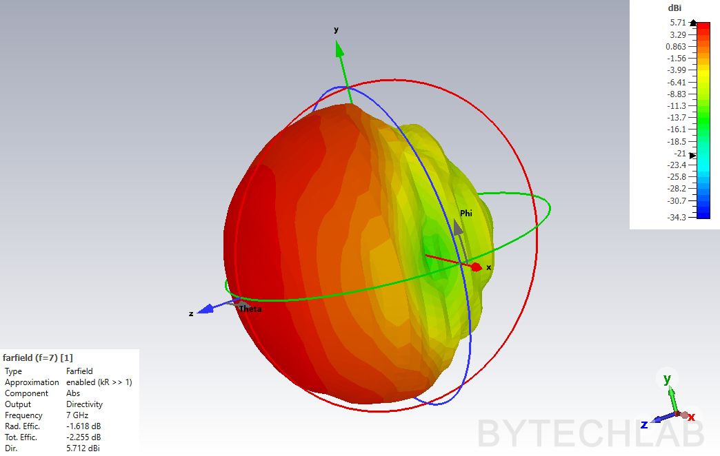
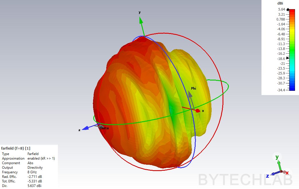
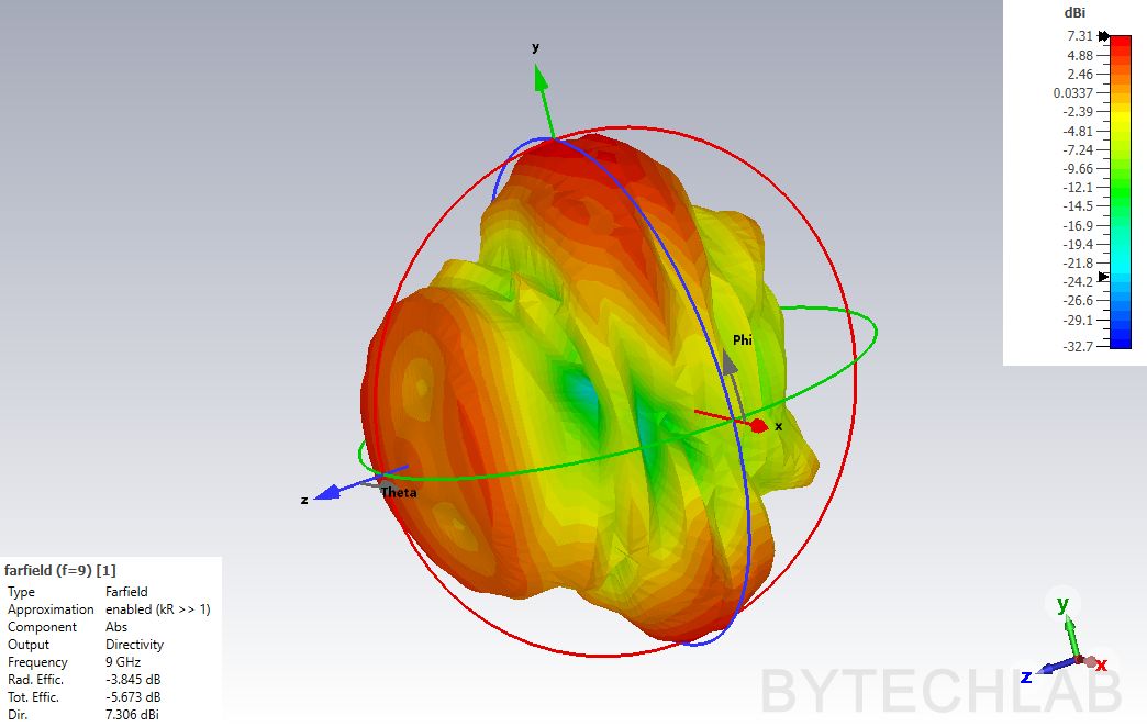
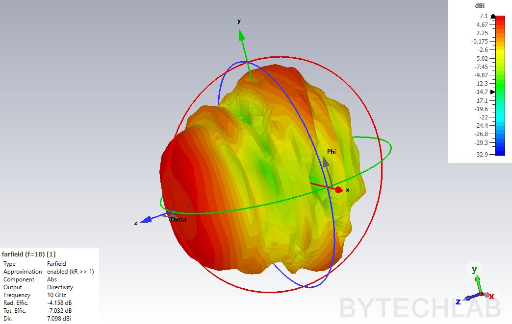
8) Does it work above 6 GHz?
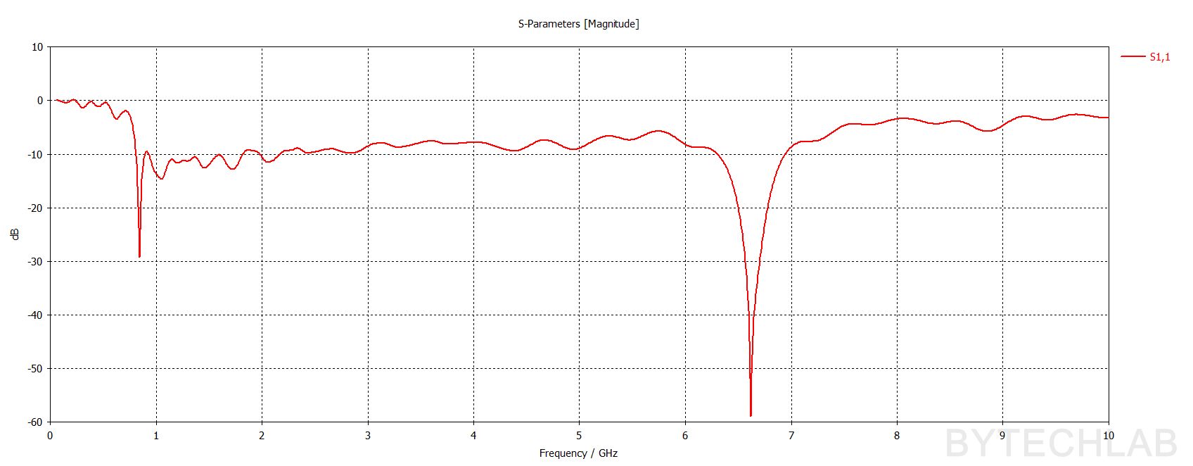
I performed additional simulations up to 10 GHz to answer this potential question. This antenna wasn’t initially simulated or designed for these frequencies, so I don’t expect much from it. The parameter degrades to ~-5 dB above 7.5 GHz, The beam starts splitting into large side lobes at 8 GHz. So I guess that if poor impedance matching isn’t a problem for someone then this antenna should be usable up to about 8 GHz.
9) Conclusions
I’m very happy with how this PCB Log Periodic Antenna turned out. The performance looks great, it is easy and cheap to make. The only thing that could be improved is the impedance matching at higher frequencies.
10) References
- [1] Colella, R.; Chietera, F.P.; Catarinucci, L. Analysis of FDM and DLP 3D-Printing Technologies to Prototype Electromagnetic Devices for RFID Applications. Sensors 2021, 21, 897. https://doi.org/10.3390/s21030897 ,LINK: https://www.mdpi.com/1424-8220/21/3/897
- [2] Abdulhameed, A.A.; Kubík, Z. Design a Compact Printed Log-Periodic Biconical Dipole Array Antenna for EMC Measurements. Electronics 2022, 11, 2877. https://doi.org/10.3390/electronics11182877 ,LINK: https://www.mdpi.com/2079-9292/11/18/2877