
I’ve got inspired by the article/post published on Hackaday some time ago : https://hackaday.com/2018/08/21/an-led-you-can-blow-out-with-no-added-sensor/ . These days everything has a microcontroller ,FPGA ,SoC or other programmable integrated circuit inside . Making such an project with use of microcontroller is too easy (you know, a few lines of code and everything works as it should). So I came up with an idea to design this circuit in a “old style”, without any programmable IC,s. That’s how this Wind Sensitive LED project was started.
The whole circuit is made with use of some op amps, transistors, passive components, one voltage comparator and of course everyone’s favorite NE555 IC. I’ve made the whole project in a few days.
Below I’ll describe how the whole thing works and how I’ve built it. I hope that you will enjoy it 🙂 .
SCHEMATICS & HOW DOES IT WORK?

I’ve simplified the whole schematic as much as I could just because I wanted to reduce number of needed components.
I will try to describe how the Wind Sensitive LED works as simple as I can.
NOTE: To show you how the whole circuit works I’ve uploaded some oscilloscope screenshots down below (they are numbered accordingly).↓↓↓↓
Anyway, let’s start!
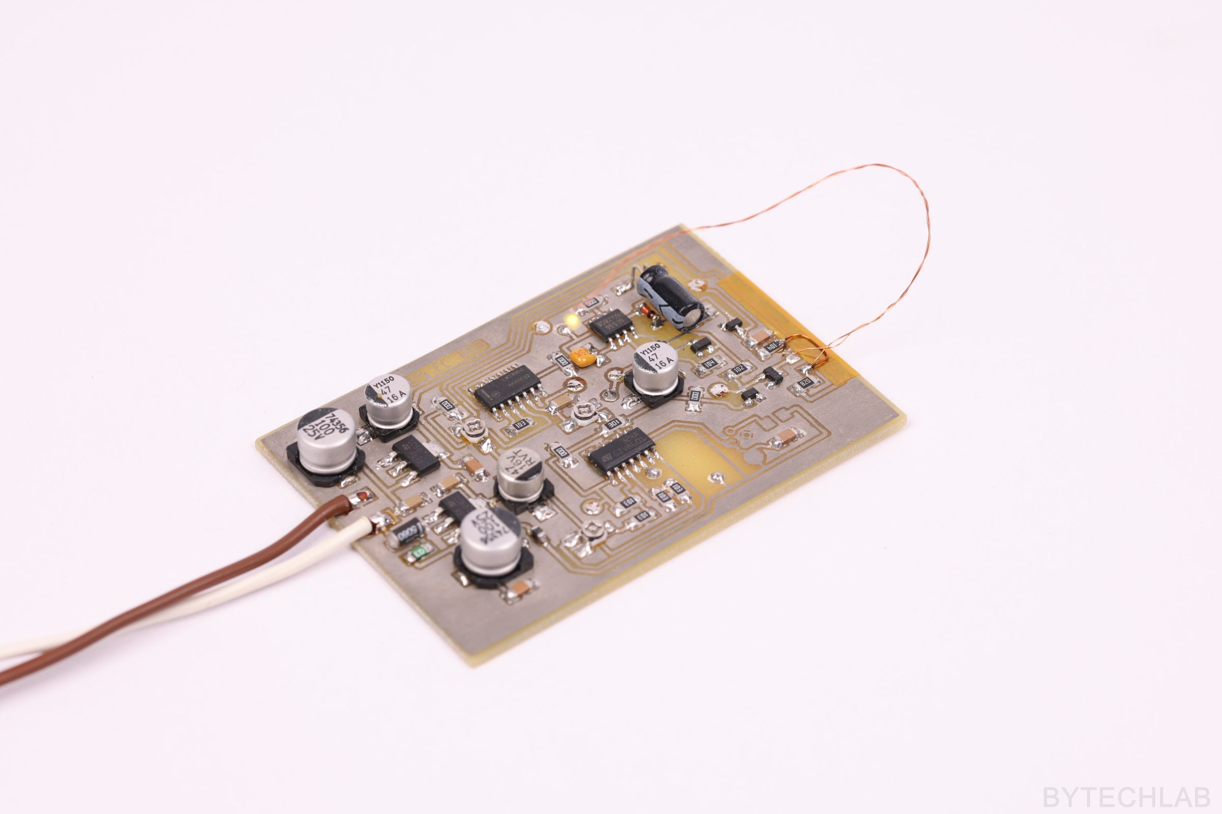
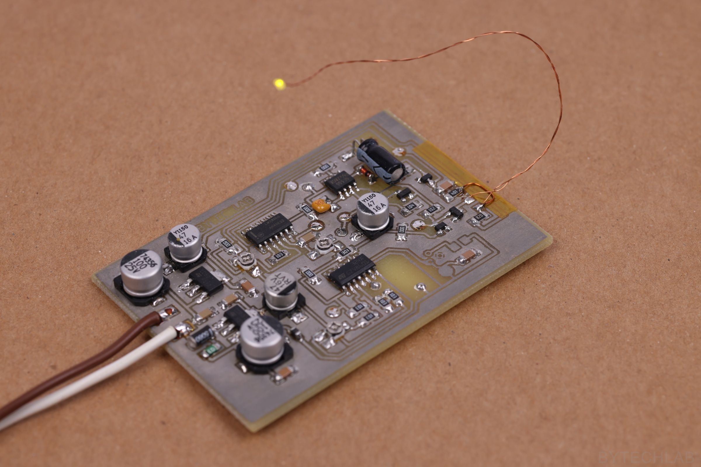
I’ve used a green LED in a 0805 SMD package which is soldered to thin (0.3 mm dia.) enamel coated copper wire.R5 is just an LED current limiting resistor, in this case it sets the current flowing through the LED to about 35 mA. This value is slightly above 20mA “standard value” just because we want the LED to heat up a little bit. When the LED heats up the voltage drop across it in the forward direction drops for a few tens of milivolts. Q3 is a standard MOSFET-N transistor in a SOT23 package (BSS123), it is normally “turned on” by the R4 pullup resistor. When the circuit detects that you are blowing at the LED Q1 pulls the gate of Q3 down to the GND switching it off almost instantly. R1 is just an base current limiting resistor value is not critical in this case a few hundreds of ohms should be fine. IC3A is a precise comparator which detects the voltage drop change, when you blow at the LED it cools a little bit and the voltage across it increases by a ~50mV or more. It crosses the threshold voltage which is being set by the R13 potentiometer.
REF-V stands for reference voltage which is provided by external voltage reference IC (for ex. LM4040CYM3). It should be “temperature compensated” just to move the trigger point with the ambient air temperature. But I found that the LED heats up that much that this compensation is not really needed (temperature of LED is much higher than ambient temperature). C9 and C10 are standard MLCC ceramic capacitors, they filter some high frequency noise just to smooth the signal a little bit. When comparator triggers it pulls down its output for a while (it is normally pulled up with a R15 resistor, this compartor needs it because it has an OD/OC output).
This small pulse (about 50µs long) triggers the NE555 IC. NE555 makes two things: it generates a ramp and it measures a time for which the LED should be switched off. This ramp is needed for fade-in effect.A ramp is being generated with use of current mirror made of 2 PNP transistors (Q4 and Q5).This current mirror acts as current source which charges the C11 capacitor. The time for which the LED stays off can be easily adjusted by changing values of R16 and C11. When NE555 output goes HIGH, C12 charges through D4 almost instantly. This charged capacitor switches on the Q3 transistor which pulls down signal from the LED which is cooled down at this moment.
When this LED is cooled down the voltage across it is slightly above the trigger point so that comparator will hold its output low all the time (LED is turned off and it is not warming up). Because of that there was an endless loop problem (comparator triggers NE555 forever). Time constant of R17,C12 and R7 allows me to adjust the signal cut-off time after the LED is switched back on (we need to wait for a while until it warms up again). Without this circuit the whole thing oscillates or doesn’t work at all. The ramp generation circuit is separated from the rest of the circuit with one op amp in voltage follower configuration (even 100k potentiometer connected directly distorted this waveform).
R12 and R14 potentiometers are used to adjust the fade in effect. Output pulse from the NE555 is being divided by R12 from 5V to about 0.7V. Ramp which has amplitude of about 5V is also divided by R14 to about 100mV. Then IC1A in differential configuration with a gain of ~1 subtracts the ramp from the output pulse (just to invert the ramp and combine these two signals together). Then this pulse is slowly switching off the Q1 transistor.When Q1 slowly switches off ,Q2 switches slowly on. The whole thing is adjusted in the way that the voltage at the collector of this transistor changes near the threshold voltage of Q2 transistor. So the whole fade-in effect (how quickly the LED lights up) can be adjusted with only two potentiometers
I’ve also added a power supply section , really nothing special, just some capacitors and LDO’s 🙂 .

OSCILLOSCOPE SCREENSHOTS

Short description of signals shown on the oscilloscope screenshots (numbers in [] brackets correspond to the screenshot number):
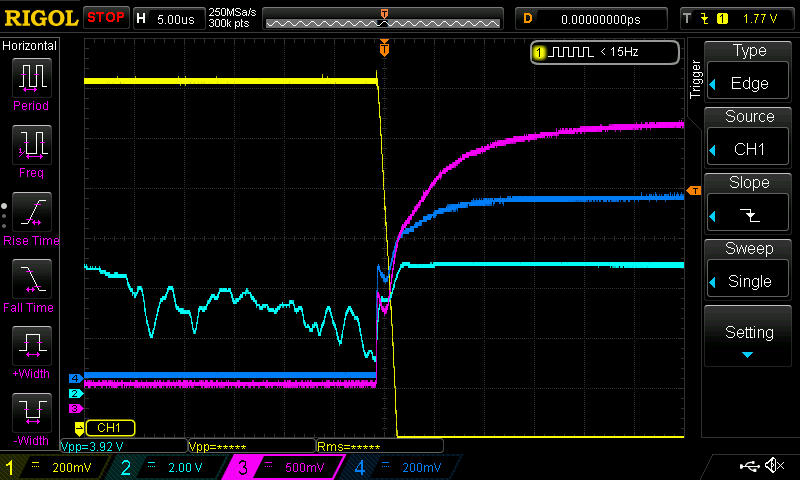
—>[1] Fade in circuit
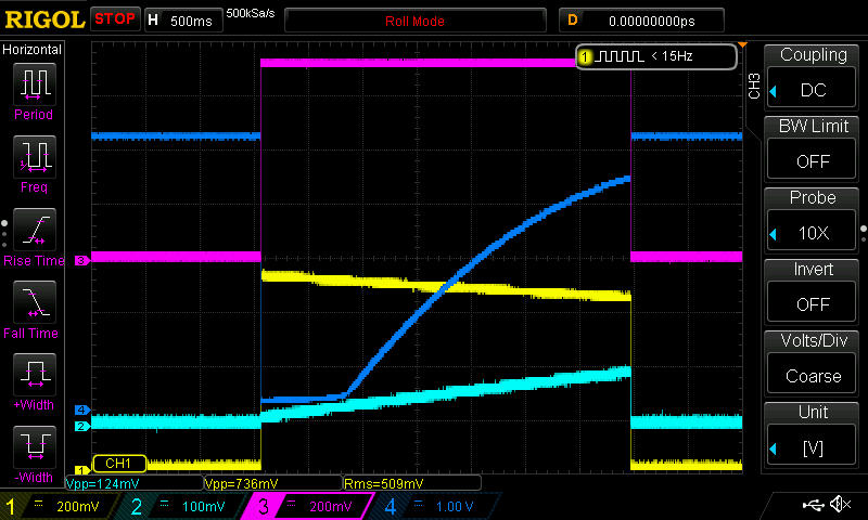
- First channel – Output of the IC1A op amp (a ramp subtracted from the NE555 output pulse)
- Second channel – Output of the R14 potentiometer
- Third channel – Output of the R12 potentiometer
- Fourth channel – Voltage at the collector of the Q1 transistor
—>[2][3][4][5] Oscillation prevention circuit
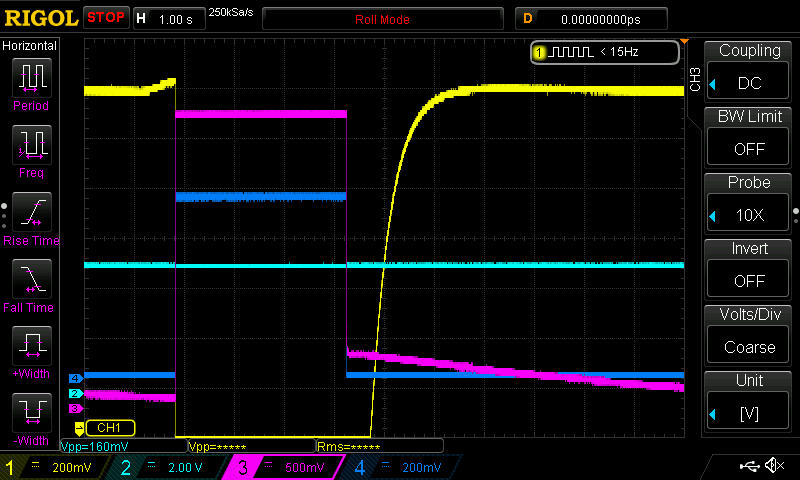
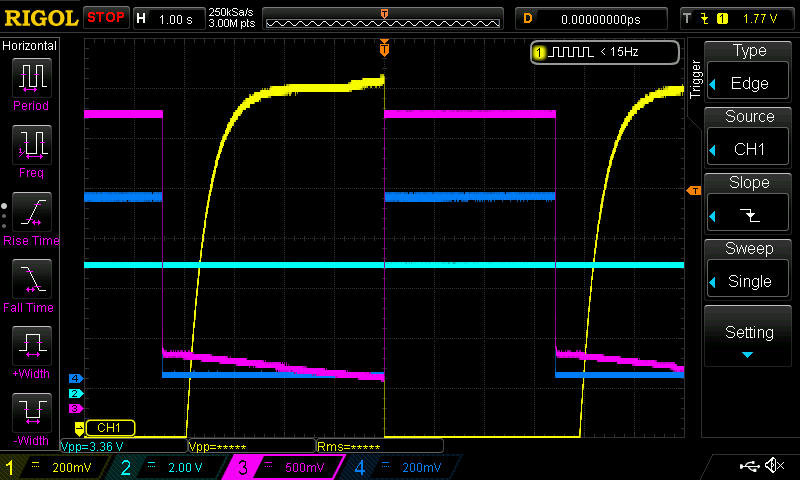
- First channel – Voltage at the collector of the Q3 transistor
- Second channel – Output of the IC3A (short output pulse)
- Third channel – Voltage at the positive terminal of the C12 capacitor
- Fourth channel – Output of the R12 potentiometer (NE555 output)
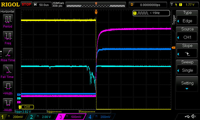
—>[6]
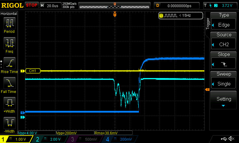
- First channel – Voltage at the positive terminal of the C11
- Second channel – Output of the IC3A (short output pulse)
- Fourth channel – Output of the R12 potentiometer
HOW IT WORKS ? – VIDEO
NOTE: The fade-in effect is not adjusted properly in this video, because of that the LED switches back on almost instantly.
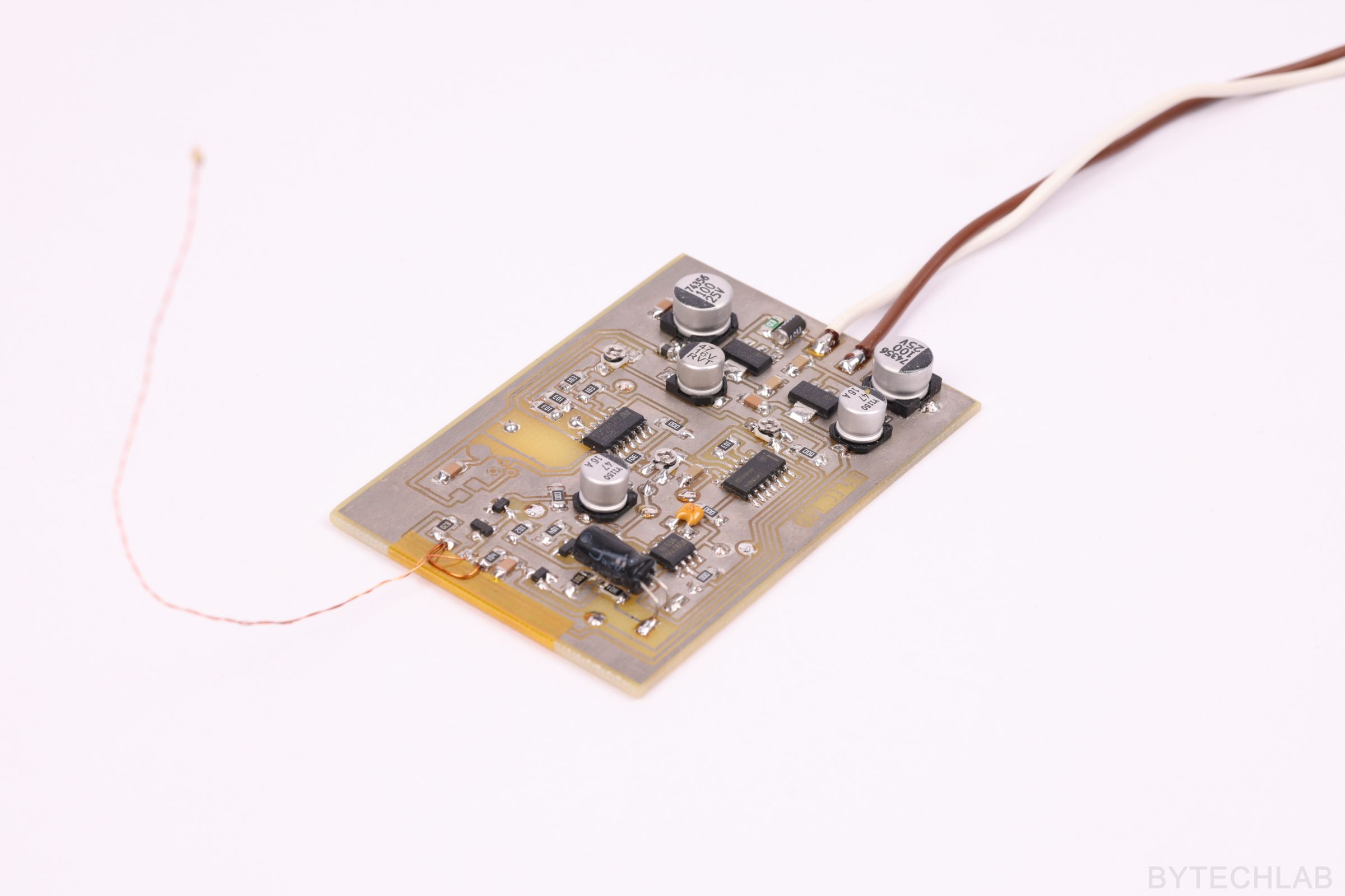
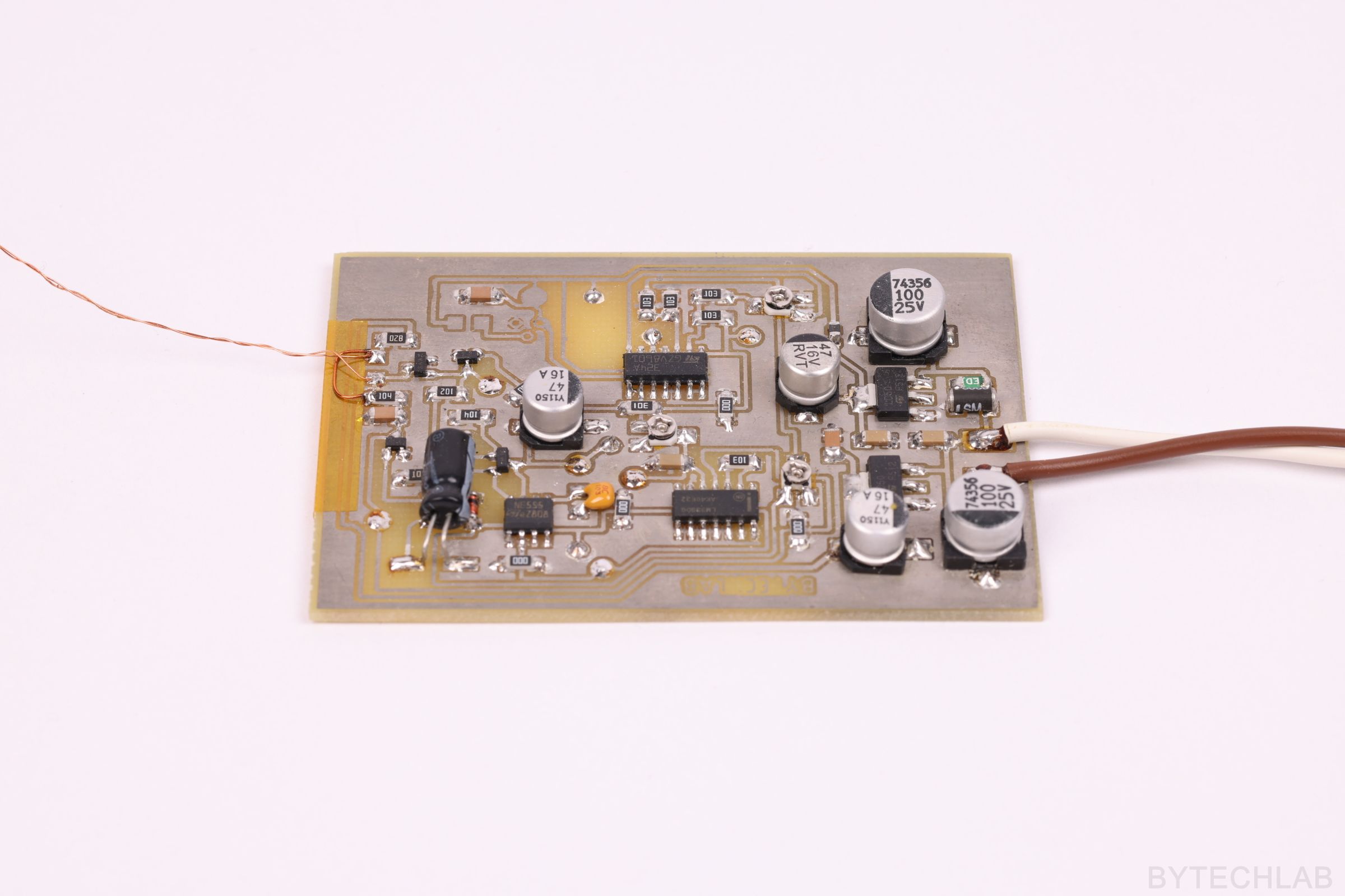
PCB DESIGN

The whole PCB was designed in Autodesk Fusion (Eagle). I’ve designed the whole thing as fast as possible, just to test the everything in a non-breadborad version (breadboards are certainly not the most reliable when considering electrical connections quality). It’s not the best PCB layout I’ve ever made,but considering that I have only one layer on this PCB it’s not that bad 🙂 .


ADDITIONAL PHOTOS
Summary
As always this post was supposed to be short ,despite efforts everything went wrong and I’ve produced a solid wall of text over here 🙂
Wind Sensitive LED is a part of other project for which I’ve already ordered PCB’s from China. When they will arrive I will write a post/short article about it.
UPDATE: You can read about this project also on: